
Plasmonic hot electron photodetector based on silica nanocone template

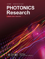
Device architecture of a plasmonic hot electron photodetector based on a silica nanocone template. Hot electrons are excited due to plasmon decay in the Au film and then travel through the TiO2 layer and eventually reach the Al electrode, forming photocurrent.
Conventional photodiode detectors made of crystalline semiconductor materials may have special requirements on fabrication affecting device integration, and their response wavelengths are limited by bandgaps, thereby causing limitation on many applications. Comparatively, plasmonic hot electron photodetectors are advantageous in these aspects. The desired response waveband can be obtained by employing appropriate materials and the response spectrum can be adjusted with designed plasmonic characteristics. Therefore, such a type of photodetectors has a broad application prospect in the field of integrated photonics. However, plasmonic hot electron photodetectors require the fabrication of nanostructures, mostly relying on electron beam lithography at present. Not only the process cost is high, but also large-area fabrication is challenging.
In order to provide a solution to this challenge, a nanocone array template is formed on a silica substrate by plasma etching using a monolayer polystyrene nanosphere mask. Metal-semiconductor-metal films are successively deposited on the template, forming an MSM structure for photodetector devices. This work is carried out by Prof. Ting Mei's group from the Shaanxi Key Laboratory of Optical Information Technology, Northwestern Polytechnical University. The related results are published in Photonics Research, Vol. 7, No. 3, 2019 (Zhiqiang Yang, et al., Silica nanocone array as a template for fabricating a plasmon induced hot electron photodetector).
The nanostructures enable surface plasmon excitation by the incident electromagnetic waves, and propagation of surface plasmon polaritons along the Au interface enhances optical absorption in the Au film. Hot electrons are generated due to plasmon decay, and those with energy larger than the Schottky barrier are emitted over the barrier into the TiO2 layer and eventually reach the Al electrode, accomplishing photoelectric conversion. Especially under an external bias, the response of the device increases, and its response peak gradually shifts red, indicating that the tunneling effect of hot electrons increases with increasing bias voltage. The researchers also use finite element simulation and related numerical theory to confirm the experimental results. In this work, costly electron beam lithography is avoided and the size of the device reaches centimeter level, which will be advantageous for the integration of hot electron photodetectors with a vast variety of optoelectronic and microelectronic devices.
Prof. Mei believes that this work not only gives a new fabrication process for plasmonic hot electron devices compatible for low-cost large-scale monolithic integration, but also provides theoretical guidance on the excitation and transport processes of hot electrons.
Further work will focus on studying nanostructures with stronger plasmon resonance on the basis of which to increase the optical absorption in metal and the efficiency of hot electron generation, and to improve the quantum efficiency of the device.
二氧化硅纳米锥模板等离子诱导热电子光电探测器
二氧化硅纳米锥模板等离子诱导热电子光电探测器结构示意图。Au膜内等离子衰变激发的热电子穿越TiO2层到达Al电极,形成光电流。
传统的光电二极管探测器由晶体半导体材料制成,可能存在制备上的特别要求从而影响器件集成,并且响应波长受限于禁带宽度,由此造成许多应用方面的限制。在这些方面,等离子诱导热电子光电探测器具有相对优势,可采用适当的材料获得所需的响应波段且其响应谱可随等离子特性调节,因而在光电子集成领域具有极为广阔的应用前景。热电子探测器需要制备纳米结构,目前大多依赖于电子束光刻技术,工艺成本高且难以大面积制备。
针对这个问题,西北工业大学陕西省光信息技术重点实验室梅霆教授的研究团队通过等离子体刻蚀单层聚苯乙烯纳米球掩膜的二氧化硅形成纳米锥阵列,再依次沉积金属-半导体-金属(MSM)薄膜,形成MSM型热电子探测器。相关研究结果发表于Photonics Research 2019年第7卷第3期(Zhiqiang Yang, et al., Silica nanocone array as a template for fabricating a plasmon induced hot electron photodetector)
由于纳米结构的存在,表面等离子可由入射电磁波激发并沿金界面传播,从而增强了金膜的光学吸收。金膜内等离子衰变产生热电子,能量大于肖特基势垒的热电子越过二氧化钛层,最终到达铝电极,实现光电转换。特别是在外置偏压下,器件的响应会增大,并且其响应峰随着偏压逐渐红移,表明随着偏压增大,热电子隧穿效应增强。研究人员还利用有限元模拟和相关数值理论对实验结果进行了验证。该器件的制备避免了成本高昂的电子束光刻工艺,并且将尺寸增加到厘米量级,这有利于热电子探测器和各种光电子器件、微电子器件的集成。
梅霆教授认为该工作不仅为低成本大规模单片集成的热电子光电器件提供了新的制备思路,并且为热电子的激发和输运过程提供了理论指导。
未来的工作将聚焦于研究等离子共振更强的纳米结构,在此基础上增加金属的吸收和热电子产出效率,以及提高器件量子效率。