
High-gain waveguide amplifiers in Si3N4 technology via double-layer monolithic integration

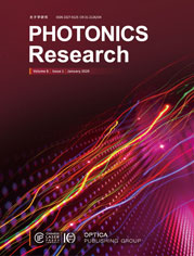
Schematic of optical waveguide amplifier die via monolithic double-layer integration platform. The cyan part indicates Si3N4 platform and the green part indicates the rare-earth-ion doped gain medium.
Active sources such as lasers and amplifiers are essential components for photonic integrated circuits (PICs) serving a myriad of applications. Silicon nitride (Si3N4) photonics, due to its low propagation loss (~0.1 dB/cm), wide transparency window (~400 nm to 2.35 µm) and good CMOS compatibility, is found to have increasing number of applications in the fields such as microwave photonics, nonlinear photonics, bio-sensing, and in technology towards autonomous driving like lidar and gyroscopes. In most applications, integration of active components onto the passive Si3N4 platform is required. The integration of III-V semiconductor optical amplifiers (SOA's) and Si3N4 by butt-coupling has led to external cavity lasers of exceptional performance. However, sophisticated assembly and packaging steps with high precision alignment are required, which significantly limits cost-effective scaling of manufacturing.
Monolithic integration of rare-earth-ion doped (RE3+) materials such as Al2O3, Ta2O5 and Te2O3 with Si3N4 show a promising approach to achieve wafer-scale active components. As compared with III-V semiconductors, RE3+ doped materials have a longer excited-state lifetime (0.1-10 ms) and less refractive index change (~10-6) induced by the excitation of the doped ions, which are beneficial for thermally and spatially stable gain.
These materials can be doped with different ions such as Nd3+, Yb3+, Er3+, Tm3+ and Ho3+ to achieve emission at different wavelengths by commonly used deposition techniques. Demonstrations have been carried out for high-speed and high internal net gain optical amplifiers and lasers. The proposed integration methodologies involve either the direct deposition of the active material onto Si3N4 elements or the sputtering into SiO2 trenches within the Si3N4 platform. Unfortunately, this inevitably increases the overall propagation loss of the photonic circuit as the active layer remains on the cladding.
To overcome this limitation, Prof. Sonia García-Blanco's team from the MESA+ Institute for Nanotechnology of the University of Twente, The Netherlands, has developed a waveguide amplifier monolithically integrated onto the Si3N4 platform via a double-layer photonic platform that supports wafer-scale manufacturing. It was published in Photonics Research, Vol. 8, Issue 10, 2020 (Jinfeng Mu, Meindert Dijkstra, Jeroen Korterik, et al. High-gain waveguide amplifiers in Si3N4 technology via double-layer monolithic integration[J]. Photonics Research, 2020, 8(10): 10001634).
In this approach, the active layer, i.e., Al2O3:RE3+, and the Si3N4 waveguides are located in two individual layers separated by a thin SiO2 film. The transfer of modes between the two layers occurs via vertically tapered adiabatic couplers that exhibit low loss, broadband behavior and high tolerance to overlay errors.
Based on the developed amplifier technology, Prof. Sonia García-Blanco believes that rare-earth ion doped materials and in particular, rare-earth ion doped Al2O3, can provide high net amplification to the Si3N4 platform, paving the way to the development of different active devices (i.e., amplifiers and lasers) monolithically integrating in this integrated photonics passive platform.
The work is impressive, particularly showing the compact spiral with gain on the double-layer active-passive integration platform. Moreover, the quality of fabrication and device performance are all excellent. Thus, this hybrid integration is important and attractive in the photonic field.
硅基氮化硅上实现单片集成的光波导放大器
波导光放大芯片示意图。淡蓝色代表氮化硅器件,绿色代表氧化铝。
有源元件如激光器和光放大器在大量光子集成电路中非常重要。由于具有低损耗、超宽带宽和良好CMOS兼容特性,硅基氮化硅光子学被快速推广至诸多应用领域,如微波光子学、非线性光子学、生物传感、自动驾驶、激光雷达以及惯导器件等领域。大多数应用场景中都急切地需要在硅基氮化硅光芯片平台上集成的有源元件。三五族半导体光放大器和氮化硅器件通过端面耦合已实现了高性能外腔激光器。然而,这种集成技术需要复杂和高精密的封测制造,因此,极大地限制了低成本、大规模的产品化量产。
在硅基氮化硅光子平台上,采用稀土掺杂材料如氧化铝、氧化钽和氧化碲等,可以实现晶圆级的有源元件单片集成。和三五族半导体材料相比,稀土掺杂材料拥有长激发态寿命和低激射所诱发的折射率变化的优点,对于增益空间和热稳定作用明显。
通过掺杂不同种类的稀土离子,比如钕、镱、铒、铥和钬等,能够覆盖从近红外到中红外的波长范围。然而,目前大多数高速和高增益应用中,这些有源材料多通过直接在氮化硅结构上面进行生长,或者在氮化硅器件上的二氧化硅包层采用挖槽的方式生长的方法得到,从而直接影响到整个光子集成电路中的低损耗特性。
为了突破这些局限,荷兰特文特大学MESA+纳米技术研究所的Sonia García-Blanco教授团队研发了能在硅基氮化硅上实现单片集成的光波导放大器技术,此项技术基于他们能够支持晶圆级制造的双层单片集成平台。该项工作发表在Photonics Research 2020第10期上(Jinfeng Mu, Meindert Dijkstra, Jeroen Korterik, et al. High-gain waveguide amplifiers in Si3N4 technology via double-layer monolithic integration[J]. Photonics Research, 2020, 8(10): 10001634)。穆进峰博士为第一作者和通讯作者。
这项研究中,利用无源二氧化硅将掺铒氧化铝和氮化硅波导隔开成独立的两层,光通过特定垂直区域耦合,从而具有低损耗、宽带宽和对光刻overlay误差超高容忍性的优点。S. García-Blanco教授认为,该工作为稀土掺杂材料尤其是稀土掺杂氧化铝,能够在氮化硅平台提供更高的增益和实现不同单片集成应用具有非常积极的意义。