
Abstract
Single-photon detectors with picosecond timing resolution have advanced rapidly in the past decade. This has spurred progress in time-correlated single-photon counting applications, from quantum optics to life sciences and remote sensing. A variety of advanced optoelectronic device architectures offer not only high-performance single-pixel devices but also the ability to scale up to detector arrays and extend single-photon sensitivity into the short-wave infrared and beyond. The advent of single-photon focal plane arrays is poised to revolutionize infrared imaging and sensing. In this mini-review, we set out performance metrics for single-photon detection, assess the requirements of single-photon light detection and ranging, and survey the state of the art and prospects for new developments across semiconductor and superconducting single-photon detection technologies. Our goal is to capture a snapshot of a rapidly developing landscape of photonic technology and forecast future trends and opportunities.
Published by Optica Publishing Group under the terms of the Creative Commons Attribution 4.0 License. Further distribution of this work must maintain attribution to the author(s) and the published article's title, journal citation, and DOI.
1. INTRODUCTION
The ability to detect individual photons with picosecond timing resolution is a key capability for emerging photonics applications [1]. The first decades of the 21st century have seen increasing interest in infrared photon counting technologies [2–5]. Time-correlated single-photon counting (TCSPC) underpins a wide range of applications, such as quantum secure communications [6], fluorescence lifetime imaging [7], positron emission tomography (PET) [8], and single-photon light detection and ranging (LIDAR) [9]. Considerable progress has been made in semiconductor single-photon detector technologies, most notably single-photon avalanche diode (SPAD) detectors [10–14]. Superconducting nanowire single-photon detector (SNSPD) technologies [15–19] have also emerged as candidates for the most demanding applications. Optical techniques such as frequency upconversion [20] and time lensing [21] also hold promise. In this Optica mini-review, we highlight progress on single-photon detectors at near-, short-, and mid-infrared wavelengths, and the impact this will have on single-photon LIDAR applications such as remote sensing [22] and autonomous vehicle navigation [23]. Furthermore, we describe relevant work on single-photon LIDAR at long range, describing different transceiver configurations and the potential advantages of short-wave infrared (SWIR) and mid-wave infrared (MWIR) operation. Advances in computational imaging techniques have allowed target reconstruction using less than one photon per pixel on average, extending the effective target distance and reducing measurement duration. The use of single-photon LIDAR imaging gives advantages in terms of surface-to-surface resolution, permitting effective reconstruction of complex scenes containing multiple surfaces.
This mini-review is intended not only as a useful resource for experts in photon counting technology and applications, but also for new researchers entering the field and potential end users of photon counting technology. The review is structured as follows: Section 2 sets out performance metrics and scaling challenges for single-photon technologies, as photon counting detector concepts are extended to longer wavelengths and scaled up to large format arrays. Section 3 surveys the promising potential and state of the art in single-photon LIDAR, highlighting recent field demonstration examples. Section 4 introduces leading candidates for single-photon detection at infrared wavelengths, from mature concepts for the near infrared (NIR) such as silicon SPAD arrays, which now offer high performance approaching megapixel formats, through the significant progress on alternative semiconductor platforms [Ge-on-Si, InGaAs, InAs, InSb, mercury cadmium telluride (HgCdTe)] for infrared photon detection, to novel contenders for mid-infrared photon detection such as SNSPDs and frequency upconversion approaches. Comparisons of the state of the art are given in Tables 1 and 2. In the concluding Section 5, we give an outlook on anticipated future developments and exciting emerging applications.
Table 1. State-of-the-Art CMOS Si SPAD Technology for Arrays
Table 2. TCSPC-Based Sensors for NIR and SWIR
2. PERFORMANCE METRICS AND SCALING CHALLENGES
A. Single-Pixel Photon Counting Performance Metrics
The first key performance metric for a single-photon counting detector [3] is the spectral range. This is the range of wavelengths that can be detected. The choice of operating wavelength is a key consideration for single-photon LIDAR systems; see Section 3. The energy per photon $E = \;hc/\lambda$ drops as the wavelength $\lambda$ increases [24], where $h$ is Planck’s constant, and $c$ is the speed of light in vacuum. The definitions of infrared spectral bands can vary among the various scientific and technical communities (telecommunications, space, astronomy, LIDAR, chemistry). For the purposes of this mini-review, we define the spectral bands as follows: NIR is defined starting at the limit of human vision at 750 nm up to a wavelength of 1.4 µm; SWIR is the spectral region from 1.4 µm to 3 µm wavelength; MWIR is the 3 µm to 5 µm wavelength band; long-wave infrared (LWIR) is the 5 to 15 µm wavelength band. For semiconductor materials, the bandgap presents an obvious threshold [25]: silicon is opaque in the visible region but becomes transparent in the NIR, so optical absorption in silicon photon detectors reduces rapidly beyond 950 nm [10]. There is therefore considerable interest in narrower bandgap materials for semiconductor photon counters that can detect wavelengths beyond the visible spectrum (Ge on Si [26], InGaAs [11], InAs [27], InSb [28], HgCdTe [29]). Moreover, spectral conversion techniques such as frequency upconversion are of great interest, allowing an elusive MWIR photon to be captured at shorter wavelengths [20].
The second key performance metric is single-photon detection efficiency. This is the probability that a photon incident on the detector triggers an electrical output pulse. In the context of single-photon LIDAR, single-photon detection efficiency is linked to the image acquisition rate. For a given photon counting detector type (see Section 4), there is usually a trade-off between achieving reasonable detection efficiency across a broad spectral range and maximizing for a particular operating wavelength (e.g., through a tailored optical cavity). Calibrated measurements of single-photon detection efficiency [3,30] rely on the availability of reliable power meters and attenuators. At NIR wavelengths and the common SWIR telecom region ${\sim}{{1550}}\;{\rm{nm}}$ this is relatively straightforward; at longer wavelengths (longer SWIR, MWIR, LWIR), calibrated single-photon detection measurements are much more challenging. It is also important to draw a distinction between system detection efficiency (from the optical input in free space or fiber) and intrinsic detection efficiency (where coupling losses have been corrected for).
The third key performance metric is the dark count rate of the photon counter. This metric is used in preference to dark current or excess noise, which are common metrics in linear mode photodetectors [31,32]. The dark count rate is the rate that the single-photon detector triggers an output pulse in the absence of any photons. For single-photon LIDAR, the pixel dark count rate contributes to noise in the raw image data. Depending on the single-photon detector type (see Section 4 for in-depth discussion), the dark count rate may depend on fluctuations in the operating temperature or electrical noise from the operating environment. The sensitivity of single-photon detectors to stray light or ambient blackbody radiation becomes an increasing challenge at infrared wavelengths, and mitigation must be considered. In semiconductor single-photon devices using the avalanche effect, the dark count rate may be increased significantly by afterpulsing, especially in high-count-rate applications [11].
The fourth key metric is the timing jitter of the single-photon detector. This is the statistical variation in the timing uncertainty between the arrival time of the photon at the detector and the output electrical pulse used to record the timing information. In the context of TCSPC [1] with ultrafast laser sources and picosecond timing electronics, the ability to time stamp the registration of incident single-photon events is ultimately limited by the detector timing jitter. This is usually quoted as a full width at half maximum (FWHM) value, but for most practical single-photon detectors, the instrument response function is not a pure Gaussian profile, and the asymmetry is more accurately modeled with additional exponential decay components. Care should be taken to distinguish FWHM timing jitter from other definitions, e.g., root mean square or standard deviation, which will give a lower value. In the context of single-photon LIDAR, the timing jitter is crucial and often the dominating factor in the range walk error [33]—the timing jitter is the limiting uncertainty in the position or measured depth of a scattering surface [34] and the ability to recognize objects: 1 ns timing jitter in free space corresponds to depth uncertainty ${\sim}{0.15}\;{\rm{m}}$; 1 ps timing jitter corresponds to a depth uncertainty ${\sim}{0.15}\;{\rm{mm}}$. Of course, one of the advantages in the TCSPC technique is that the depth resolution can be improved by averaging over many laser pulses. This allows the depth resolution to be reduced to a level well below that determined by the system jitter, such that sub-mm resolution can be routinely achievable with modest acquisition times [34]. However, this requires a trade-off of depth resolution with acquisition time, and also the possible consideration of the longer-term stability of individual LIDAR system components.
The maximum count rate of a photon counting detector is typically limited by the recovery time of the single-photon detector, although in some instances, the dead time of the timing electronics also plays a role. Effects such as afterpulsing [35] can necessitate a longer recovery time to be enforced for efficient single-photon measurement. Both of these factors have a bearing on image acquisition rate in single-photon LIDAR.
The final parameter that can vary widely across photon counting technologies is the operating temperature. This can vary between room temperature or above, down to sub-Kelvin temperatures [5]. This has a significant impact on the practicality and footprint of photon counting detectors deployed in single-photon LIDAR systems.
There are also subtle effects that can be exploited in single-photon imaging scenarios—the ability to determine photon energy and photon number resolution [36] has been explored and can be achieved through some novel detector types. Polarization sensitivity in detectors can also potentially be exploited in single-photon LIDAR systems for improved signal-to-background ratios [37].
B. Scaling Challenges for Photon Counting Arrays
Now let us consider expanding upon the single-pixel single-photon counting detector metrics in Section 2.A to include key characteristics for photon counting arrays for high-timing-resolution single-photon LIDAR. In principle, the use of single-photon detector arrays will allow the simultaneous acquisition of depth data across an entire optical field of view (or part of the field of view), opening up opportunities for rapid measurement of static targets and leading to 3D reconstruction of moving objects.
An obvious consideration is the maximum number of pixels achievable and the overall active area of the photon counting array. Increasing these parameters will boost the photon detection rate and thus the image acquisition rate. The active area divided by the total area of the array is the fill factor. A typical single-photon detector array will have a fill factor of less than one; there must be some gaps between pixels, and in a planar geometry, wiring must be routed between pixels, reducing the fill factor. This difficulty can be mitigated by using multiple wiring layers and through-substrate vias. Moreover, optical coupling strategies such as microlens arrays can capture incident light and focus it effectively onto widely spaced low-fill-factor pixels.
As photon counting arrays scale up to large format focal plane arrays and cameras, cross talk between pixels becomes a significant consideration. This will contribute to noise and artifacts in the overall image on top of the dark count rate per pixel. As wiring becomes more dense, electrical interference when pixels are activated can be a concern. Also, defective hot pixels can degrade the performance of neighboring pixels. In semiconductor avalanche-diode-based photon counting arrays, the re-emission of photons following an avalanche event can trigger cross talk that has to be mitigated, for example, by etching trenches between neighboring pixels [38] either to trap re-emitted photons by total internal reflection or to insert an absorbing barrier between pixels.
As the number of pixels increases, the challenge of data readout becomes daunting, and there are trade-offs between maximum frame rate and preserving accurate timing resolution within a finite data bandwidth. For true TCSPC, precision time stamping of photon arrivals and tagging arrival events to specific pixels is the key requirement. If all parameters for the counting array are known in combination with the illumination and collection optics, then the fundamental limits of depth imaging using SPAD arrays can be established [39].
The characterization of large arrays and determining fabrication yield is a considerable technological challenge. Even in silicon with advanced CMOS processes, no process has perfect yield. For infrared photon counting arrays, novel materials and evolving fabrication processes are being employed. Identifying defective pixels is a key requirement and a major challenge for manufacturers; pixel-by-pixel characterization of single-photon performance is clearly not practicable as photon counting arrays scale up from kilopixels to megapixels.
An important factor in the selection and deployment of photon counting arrays by end-users is the power consumption of the array. The energy consumed per event is a useful metric. The energy consumption due to detector cooling is yet another vital consideration. For many novel infrared single-photon counting detector types, both superconductors and novel semiconductors, these cooling requirements can be onerous, preventing reduction in the size, weight, and power (SWaP) and cost of the overall photon counting system. Of course, such system considerations should also consider the available source technology, which tends to utilize laser diodes in the NIR, and often diode-pumped solid-state and fiber lasers in the SWIR region [40–42].
3. LONG-RANGE SINGLE-PHOTON LIDAR
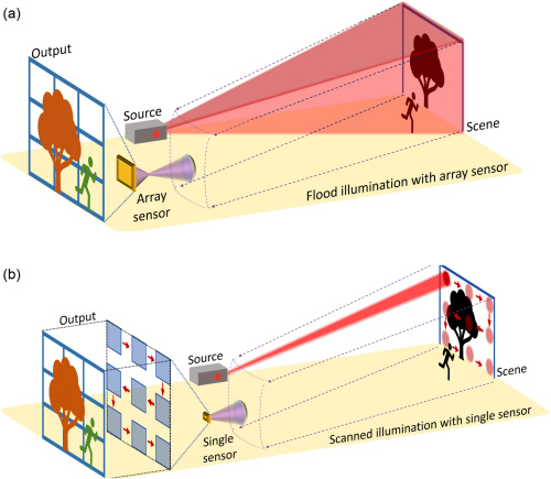
In the past decade, quantum technologies have entered mainstream discussion of emerging technological priorities in major economies across the globe [43–46]. Quantum computing is a coveted long-term prize, but nearer-term impacts are more likely in domains such as sensing and imaging enhanced by quantum technology. Single-photon detectors have been specifically identified as an important underpinning capability [47]. LIDAR—also sometimes referred to as laser detection and ranging (LADAR)—is analogous to radio detection and ranging (RADAR, radio and mm wave) translated to the optical spectral domain. A canonical time-of-flight LIDAR system sends out a short laser pulse (typically sub-nanosecond duration) and detects the return time of backscattered light from the target object inferring the target distance from this timing information. By using a detector array, as shown in Fig. 1(a), a 3D reconstruction of the object is possible when full-field illumination is used in a flash LIDAR configuration. Alternatively, the scanning of the object can be performed with a single-pixel detector and narrow field of view illumination, as shown in Fig. 1(b), using a variety of scanning configurations. There is huge interest in the area of compact illumination and optical scanning for LIDAR, using a toolkit of techniques from nanophotonics, micro electronic mechanical systems (MEMS), and integrated photonics [48,49]. The intrinsic time gating of the time-of-flight LIDAR approach allows precise imaging even in the presence of intervening obscurants and clutter (e.g., imaging of a vehicle concealed behind trees and foliage).

Fig. 1. Examples of imaging LIDAR configurations. (a) Flash LIDAR configuration using an array sensor and full-field illumination (a bistatic system is shown, with source and sensor separated). (b) Scanning LIDAR approach where the source is scanned and an individual sensor is used. (In this illustration, a bistatic configuration is shown; however, a monostatic scanning configuration is often used with a common transmit and receive axis).
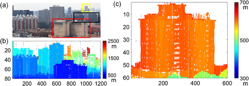
Fig. 2. Single-photon LIDAR depth profiles taken at a range of greater than 600 m using a 100-channel Si SPAD detector system in scanning configuration. The operational wavelength is 532 nm. (a) Visible-band photograph of scene. (b) Reconstructed depth image of the city scene. (c) Detailed depth profile of the subsection of the scene within the red rectangle in (a). Further details in Z. Li et al. [60]. Figure reproduced with permission of Optica Publishing Group.
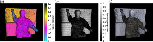
To achieve maximum range with constrained laser power, a single-photon counting detector is clearly desirable. Early pioneering photon counting ranging studies were carried out in the context of space and satellite telemetry [50–52] and satellite-borne imagers for Earth observation [53–55]. Over the past decades, photon counting LIDAR has emerged as a technological area of increasing importance and widening interest: at visible, NIR, and SWIR wavelengths, sophisticated systems are under development for future commercialization [13,56]. The achievable depth resolution is governed by a combination of the overall system timing jitter (a convolution of jitter contributions mainly from the single-photon detector, laser source, and timing electronics) and the level of photon return. Hence, excellent depth resolution, far lower than that determined by the system jitter alone, can be achieved by a longer duration acquisition or a higher illumination power level, as detailed by Pellegrini et al. [34]. The transceiver system jitter contributions play the dominant role in determining the overall system temporal response, and factors such as turbulence or atmospheric scatter can generally be considered as having a negligible effect on timing response [57]. However, LIDAR systems based on the most highly advanced low-jitter detector technology may make this assumption less valid [58]. Much of the earlier single-photon LIDAR imaging was initially performed in the visible and NIR due to the ready availability of Si-based SPADs [9], and was used in scanning configurations [59], in multiple detector formats [60], or in combinations of these configurations [61,62]. The multibeam, multiple Si SPAD detector format of Li et al. [60] demonstrated good long-range performance when used with 100 individual beams and detectors. Figure 2 presents 3D LIDAR imaging at ranges greater than 600 m when this sensor is operated in conjunction with a scanning transceiver. In terms of long-range LIDAR imaging, complementary metal–oxide–semiconductor (CMOS) SPAD detector arrays have been used in several significant demonstrations of LIDAR imaging. These examples include demonstrations in both TCSPC mode for automotive applications [63] and for foliage penetration [62], but also in range-gated mode for rapid 3D imaging [64]. The large pixel formats available with CMOS SPADs can be used effectively in data fusion approaches with other sensor modalities. One example by Chan et al. [65] was the use of single-photon LIDAR from a CMOS SPAD detector array with visible-band passive imagery to reconstruct 3D color scenes at distances of 150 m. An example is shown in Fig. 3.
Fig. 3. Example of data fusion of a 3D image from a CMOS SPAD detector array and passive imagery of a scene at 150 m range. (a) Retrieved depth information from a SPAD detector array. (b) Intensity information from the SPAD overlaid on top of the retrieved depth information. (c) Intensity information from a color camera overlaid on top of the retrieved depth information [65]. Figure reproduced with permission of Springer Nature publishing.
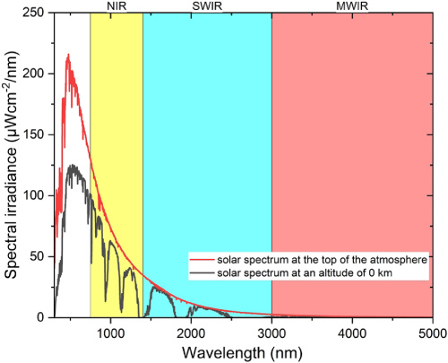
Fig. 4. Solar irradiance versus wavelength at sea level (red) and in the upper atmosphere (blue). MODTRAN simulation [86]. The following spectral bands beyond the visible wavelength range are denoted by the shaded regions: near infrared (NIR), yellow; short-ware infrared (SWIR), cyan; mid-wave infrared (MWIR), red.
Although there are several potential advantages of SWIR operation of single-photon LIDAR imaging systems, CMOS SPAD detectors have been used much more extensively in LIDAR imaging demonstrations [13]. This is because NIR CMOS SPAD arrays (Section 4.A.1 and Table 1) [64,66–71] are significantly more advanced than SWIR alternatives (Section 4.A.2–4.A.4, Section 4.B, Section 4.C, and Table 2) [72–79], allowing considerably larger pixel formats and generally improved readout capabilities. This can allow impressive performance in terms of, for example, high-speed sensing of moving objects [80,81]. For example, Gyongy et al. [80] used hybrid mode imaging and guided upsampling approaches to capture and display single-photon images at 1050 frames per second over short-range indoor scenes with moving targets. In this work, the sensor reports alternate intensity images and depth information that can be combined to generate high-resolution depth images at high frame rates. Another emerging area of interest for CMOS SPAD arrays is in the integration of mosaic optical filters where individual spectral filters are used at the pixel level, for reconstruction of color images using single-photon data. A recent example utilizes metamaterial mosaic filters integrated with a SPAD array to utilize individual bandpass optical filters on each pixel to show full color reconstruction [82]. Also recently, Ogi et al. [83] have used more traditional red, green, blue (RGB) filter approaches for color reconstruction with CMOS SPAD arrays. CMOS SPADs have been shown to be also effective in demonstrations of light-in-flight imaging [84] and imaging around corners [85].
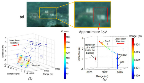
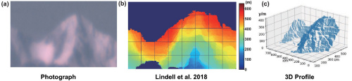
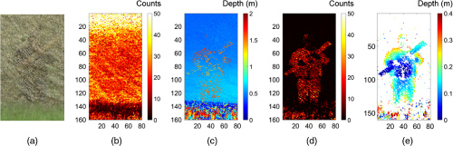
There are several potential advantages of SWIR and indeed MWIR LIDAR operation compared to NIR operation: (i) improved atmospheric transmission; (ii) increased maximum permissible exposure levels of laser illumination at wavelengths greater than 1400 nm; (iii) reduced solar background levels, and (iv) reduced attenuation for some types of atmospheric obscurants. Figure 4 illustrates the contrast in solar irradiance versus wavelength at sea level and in the upper atmosphere using MODTRAN simulation software [86]. SWIR single-photon scanning systems have been used effectively for long-range imaging applications, and these potential advantages have provided motivation for kilometer-range single-photon LIDAR demonstrations using scanning transceivers at $\lambda \sim{{1550}}\;{\rm{nm}}$ using both InGaAs/InP SPADs [87] and SNSPDs [88]. An early example is by Pawlikowska et al. [89] where a scanning transceiver incorporating an InGaAs/InP SPAD detector mapped features at distances up to 10 km. A depth intensity image of a building at a range of 8.8 km is shown in Fig. 5, which was taken with an average laser illumination of 10 mW in daylight conditions. This led to further demonstrations, including significant work in LIDAR imaging at 45 km range by Li et al. [90]. To date, the longest-range single-photon LIDAR imaging is over distances of 200 km by Li et al. [91]. In this work, mountains were mapped, as shown in Fig. 6. Although super-resolution over long distances has been demonstrated in the lateral axis [93], one of the major advantages of single-photon LIDAR is the surface-to-surface resolution, with mm-dimension separations being resolved over long distances [94]. More complex scenes have also been investigated that rely on the depth resolution afforded by the single-photon approach. For example, Tobin et al. have demonstrated the reconstruction of object profiles obscured by camouflage [95]. Figure 7 illustrates that the depth profile of a human figure can be extracted from behind camouflage, with the use of selected single-photon timing data and a routine pixelwise analysis.
Fig. 5. Example of scanning SWIR single-photon LIDAR imaging. (a) Visible-band image of a residential building taken with an ${{f}} = {{200}}\;{\rm{mm}}$ camera lens. (b) Depth intensity plot of the building imaged with ${{32}} \times {{32}}$ scan points over a range of 8.8 km. (c) Depth plot of the building imaged with ${{32}} \times {{32}}$ scan points over a range of 8.8 km; side view of the target [89]. Figure reproduced with permission of Optica Publishing Group.
Fig. 6. Reconstruction results of a mountain scene over a range of 201.5 km using SWIR single-photon LIDAR [91]. (a) Visible-band imaged photograph. (b) Reconstructed depth result using algorithm by Lindell et al. [92] for data with signal-to-background ratio $\sim {0.04}$ and mean signal photon per pixel $\sim{3.58}$. (c) 3D profile of the reconstructed result. Figure reproduced with permission of Optica Publishing Group.
Fig. 7. Analysis of a scene with an actor holding a wooden plank across his chest and standing 1 m behind camouflage netting at a range of 230 m in daylight conditions. (a) Photograph of the scene, showing the actor holding a wooden plank behind the camouflage. (b), (c) Intensity and depth profiles of the target scene using all the collected single-photon LIDAR data. (d), (e) Intensity and depth profiles after time gating to exclude all data except those with a 0.6 m range around the target location. The pixel format used in the depth and intensity profiles is ${{80}} \times {{160}}$ [95]. Figure reproduced with permission of SPIE publishing.
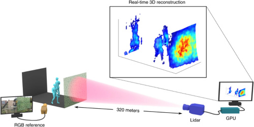
In all these impressive SWIR single-photon range and intensity profiles, there are numerous computational imaging approaches that can significantly reduce the average number of photons per pixel required to form image depth and/or intensity reconstruction of sufficient high quality to have significant value for applications, including Kirmani et al. [96], Shin et al [97], Rapp and Goyal [98], Altmann et al. [99], and Lindell et al. [92]. Nonetheless, there remain challenges with the long acquisition time taken for the optical scanning process, which is particularly evident if reconstructions of moving scenes are required. Inevitably, full-field or part-field images taken with SWIR detector arrays [100] can overcome some of these issues, and this approach has been investigated for outdoor, long-range scenes by several groups [101,102]. This approach is vital for rapid measurement of moving scenes. One particularly notable example is the work by Tachella et al. [101], where depth and intensity profiles were reconstructed from measurements at 320 m range using full-field illumination of moving human figures in a complex daylight scene, again behind camouflage; see Fig. 8. The demonstrations consisted of using a ${{32}} \times {{32}}$ InGaAs/InP SPAD detector array to recreate moving scenes at 50 frames per second, with each frame being processed in less than 20 ms duration. In this example, an average illumination power of 220 mW at $\lambda = {{1550}}\;{\rm{nm}}$ was used, which was considered eye-safe using this optical configuration. The computational imaging was performed by using a statistical model combined with scalable computational tools from the computer graphics industry, allowing multiple surfaces to be identified in a given pixel and for a super-resolved ${{96}} \times {{96}}$ image to be displayed. Other work on moving images includes the use of a similar SWIR optical transceiver to reconstruct scenes in the presence of atmospheric obscurants, where optical backscattering causes a non-uniform background level that poses a particular challenge in these LIDAR measurements. In [103], Tobin et al. measured scenes at five attenuation lengths between transceiver and target at 150 m range, and reconstructed moving targets at 50 m range, using a fast and robust statistically based processing algorithm. Later, Jaing et al. [104] used an InGaAs/InP SPAD array and 1550 nm wavelength illumination to detect scenes through low levels of atmospheric obscurants at kilometer range. This work follows other single-photon LIDAR demonstrations using scanning SWIR sensors [104] and work using CMOS SPAD arrays applied to static scenes. The field of depth imaging through atmospheric obscurants [105–107] is an application in which SWIR single-photon imaging arrayed format detectors may have advantages due to improved transmission in this spectral band and allowing more rapid data acquisition and image reconstruction.
Fig. 8. Schematic diagram of a SWIR single-photon 3D flash imaging experiment. The scene consists of two people walking behind a camouflage net at a stand-off distance of 320 m from the LIDAR system. An RGB camera was positioned a few meters from the 3D scene and used to acquire a reference video. The proposed algorithm is able to provide real-time 3D reconstructions using a graphics processing unit (GPU). As the LIDAR presents only ${{32}} \times {{32}}$ pixels, the point cloud was estimated in a higher resolution of ${{96}} \times {{96}}$ pixels. The acquired movie is shown in [101]. Figure reproduced with permission of Springer Nature publishing.
For free-space single-photon LIDAR, SWIR operation has clear potential benefits (Fig. 4), in terms of both atmospheric penetration and avoiding solar background. Also, for civil use (e.g., in autonomous vehicle navigation and sensing for road and rail), eye safety governed by maximum permissible exposure standards is improved at wavelengths greater than 1400 nm. For security and defense, longer wavelengths allow the illumination signal to be less readily detected. SWIR LIDAR approaches also allow the detection of aerosol layers at long range, a good example being presented by Yu et al. [108], where cloud layers were detected at an altitude of 12 km. Undoubtedly for wide adoption, detection system SWaP and cost are likely to be important factors in whether photon counting receivers are chosen. For specialist mobile scientific or security applications (e.g., airborne, satellite single-photon LIDARs) the SWaP, performance, ruggedness, and reliability of systems are also critical considerations.
4. SINGLE-PHOTON DETECTORS FOR LONG-RANGE LIDAR: SURVEY OF STATE OF THE ART AND PROSPECTS
The main detector types under consideration for infrared single-photon LIDAR are SPADs and SNSPDs. The device architectures are illustrated in Fig. 9 (below) and comparisons of recent developments are given in Tables 1 and 2 (above).
Fig. 9. Single-photon detector technologies for infrared single-photon LIDAR, with spectral coverage for each detector type indicated. (a) Schematic diagram cross section of a Si-based SPAD detector. The design is a homojunction. (b) Schematic diagram cross section of a Ge-on-Si structure, illustrating optical absorption in the Ge layer, and multiplication in the intrinsic Si layer. (c) Schematic diagram cross section of an InGaAs/InP SPAD detector; the absorption is in the narrow-gap InGaAs and the multiplication in the wider gap InP layer. In both (b) and (c), the charge sheet is used to alter the relative electric fields in the absorption and multiplication layers. (d) Schematic illustration of SNSPD architecture for near-unity efficiency at 1550 nm wavelength and optical micrograph of chip with single-pixel detector [109]; (d) reproduced with permission of Optica Publishing Group.
A. Semiconductor Single-Photon Avalanche Diodes
1. Si SPAD Arrays
The most widely used photon counting detectors are based on the semiconductor SPAD architecture [10]. The heart of the device is an avalanche photodiode (APD) (centered on a ${\rm{p}} {-} {\rm{n}}$ or ${\rm{p}} {-} {\rm{i}} {-} {\rm{n}}$ junction). The diode is reverse-biased above the breakdown voltage, and this operating regime is known as Geiger mode. Carriers generated by photon absorption undergo avalanche gain, triggering a macroscopic breakdown of the diode junction [110]. To exploit this effect in a practical device, the avalanche must be arrested, and the device reset by a quenching circuit. Compared with a conventional APD, the SPAD is a threshold device with a digital output, allowing stable operation with reliable performance over a range of operating temperatures and in the presence of electrical noise. Si SPAD devices offer high-efficiency photon counting from UV to NIR wavelengths. A typical Si SPAD device architecture is illustrated in Fig. 9(a). The UV performance is limited by high levels of absorption of high-energy photons near the surface of the device; the long-wavelength cutoff is due to the photon energy dropping below the bandgap of the silicon semiconductor, preventing absorption.
Silicon SPAD arrays have undergone rapid development and have been deployed in numerous single-photon LIDAR applications [84,111–114]. Detector elements can be integrated directly with quenching circuitry. Cross talk from photon re-emission is mitigated by deep trench isolation between pixels. The most advanced Si SPAD arrays for single-photon LIDAR using TCSPC tend to offer in the range of 10–100 kilopixels, but these large arrays have limited bandwidth available to stream time-tagged event data from the detector array. One approach used for increasing the throughput of data from these SPAD arrays is to use a range-gated SPAD for timing measurement, where only the number of photons is recorded within a pre-determined detector gate duration and delay. While this approach will not utilize the full picosecond resolution possible in TCSPC, it will allow a much greater rate of recorded photon events in a large pixel format SPAD detector array, while still allowing depth resolution of approximately tens of centimeters. This range-gated mode of operation has now been incorporated in “megapixel” SPAD detector arrays fabricated with low dark counts and minimal cross talk [115,116]. Recently, Canon Inc. developed a SPAD array with a record high pixel count of 3.2 megapixels [64] for low-light color imaging. A comparison of Si SPAD array sensors [64,66–71] reported in the literature as of June 2023 is shown in Table 1 (above). This table outlines the large SPAD detector arrays currently described in the literature, and work is continually ongoing in optimizing the individual SPAD and overall array performance via approaches such as pixel miniaturization for highly efficient and low-noise compact arrays [71,117–119], as well as very high-speed performance as a result of low jitter [120,121] and dead time [122].
2. Ge-on-Si SPADs
To extend single-photon detection deeper into the infrared, SPAD devices based on narrow bandgap semiconductors have been employed. Several decades ago, Ge SPADs were evaluated in photon counting applications [123] but not widely adopted. Some early experiments were performed using devices incorporating a ${\rm{Si}}/{{\rm{S}}_{1 - x}}\;{\rm{G}}{{\rm{e}}_x}$ multiple quantum well absorber layer adjacent to an all-Si multiplication layer; however, this work was hampered by low levels of SWIR absorption and limited spectral coverage [124]. Since then, improvements in Ge-on-Si technology [125] have given rise to a new generation of Ge-on-Si that can be manufactured by adapting silicon foundry fabrication processes [126]. The generic layer structure of a Ge-on-Si SPAD is shown in Fig. 9(b), where a µm-dimensioned thickness Ge absorber is grown on a Si multiplication layer. Photons absorbed in the Ge layer create electron–hole pairs, and electrons drift in the electric field to the Si multiplication layer to initiate the avalanche process. Ge-on-Si SPADs give promising photon counting performance in the SWIR in waveguide integrated [127] and planar geometries [72,73,128]. The wavelength cutoff for single-photon counting is ${\sim}{{1500}}\;{\rm{nm}}$ (caused in part by the necessarily reduced operating temperature), but efforts are underway to improve efficiency at the key 1550 nm wavelength telecom band, and towards room temperature operation. Initial measurements also have demonstrated lower afterpulsing compared to InGaAs/InP SPADs under similar operating conditions at lower temperatures, which could prove to be a critical performance criterion in single-photon LIDAR applications [72]. Ge-on-Si SPADs have been demonstrated in proof-of-principle single-photon LIDAR at short ranges [74]. An exciting prospect is that through the addition of Sn, Ge(Sn)-Si SPADs could potentially extend the single-photon performance to beyond 2 µm wavelength [129].
3. InGaAs/InP SPADs
To date, the best results for SPADs tailored to telecommunications wavelengths ($\lambda = {{1310}}\;{\rm{nm}}$ and 1550 nm) have been achieved with InGaAs/InP separate absorption and multiplication devices [11,130]. As shown in Fig. 9(c), an InP multiplication layer is grown on top of an InGaAs absorption region, and SWIR photons are absorbed in the InGaAs layer. The ${{\rm{p}}^ +}$ layer in typically formed by multiple in-diffusions of Zn dopant, shaped to avoid edge breakdown. Typically, floating guard rings are also used (not shown in diagram). The photo-generated holes drift towards the wider gap InP region, encountering the valence band discontinuity between the narrow gap InGaAs and wide gap InP layers. An intermediate gap InGaAsP layer is required to assist hole transport across this discontinuity. InGaAs/InP SPADs have demonstrated single-photon sensitivity across the 1000–1600 nm wavelength range and typically have shown detection efficiencies of 20% to 30% at $\lambda = {{1550}}\;{\rm{nm}}$ [131–133], although improved detection efficiencies, 50% and higher, have been demonstrated using GHz gating [134–136] or thick InGaAs absorption layers [137,138]. A great deal of research has focused on ways of quenching the devices to reduce the deleterious effects of afterpulsing and to allow higher-temperature operation [139–144]. As discussed in Section 3, single-pixel InGaAs/InP SPAD single-photon imaging systems have been used to demonstrate long-range depth imaging [87] up to 200 km distance [91] and imaging through obscurants [105]. InP-based SPAD arrays have also been developed for single-photon LIDAR at 1064 nm using wider gap InGaAsP absorbers [145]. As described above, InGaAs/InP SPAD arrays have advanced considerably to ${\gt}$kilopixel size [75,100]. InGaAs/InP SPAD cameras have been used in demonstrations of single-photon LIDAR at 1550 nm wavelength [103,105]. This technology is now under commercial consideration for SWIR single-photon LIDAR for autonomous vehicles.
4. Mid-Wave Infrared (3–5 µm): from Avalanche Photodiodes to SPADs
In principle, extending SPAD performance beyond $\lambda = {1.6}\;{{\unicode{x00B5}{\rm m}}}$ is a matter of selecting and engineering an appropriate semiconductor materials system. A variety of compound semiconductor systems exist and have been under close consideration for SWIR and MWIR detection applications for many decades, for example, InAs, InSb, and HgCdTe [146–149]. In practice, the materials engineering challenges are formidable. In this domain, end-users must consider carefully whether the reported work is an APD operating at low light levels, versus genuine photon counting with a Geiger-mode SPAD suitable for TCSPC applications. Semiconductor APD or SPAD devices for MWIR are operated at low temperatures (77–130 K is typical) requiring liquid nitrogen or cryocoolers.
HgCdTe [also known as MerCad telluride (MCT) or CMT] is an established ternary compound semiconductor. HgCdTe is prized for MWIR and LWIR applications as the bandgap can be tuned over a very wide energy range (from semi-metallic up to 1.6 eV hence covering wavelengths up to 30 µm). As the constituent elements are toxic, HgCdTe may be subject to a future worldwide phaseout of industrial manufacturing. HgCdTe MWIR APD focal plane arrays with very low excess noise have been developed by several manufacturers worldwide. There are now HgCdTe SPAD arrays integrated with readout integrated circuits (ROICs) in formats such as ${{2}} \times {{8}}$ [29] or quadrant [148]. Instead of using Geiger mode operation as is the case for Si SPAD arrays, these HgCdTe APD arrays utilize the large avalanche gains from HgCdTe APDs. Although high photon detection efficiency values were reported at 1.55 µm wavelength [29,150], their efficiency is likely to be reduced at MWIR and LWIR due to notable changes in photogenerated carrier profiles. The lowest excess noise is achieved under pure electron injection conditions, which are increasingly difficult to maintain, as increasing the operational wavelength leads to photon absorption being distributed across the entire high-field region.
III-V alternatives to HgCdTe APDs (such as InAs and InSb) currently exhibit performance below those of HgCdTe APDs. There has been no InAs or InSb SPAD reported to date. InAs APDs detect up to 3.5–4.0 µm (at 77 K and 300 K, respectively) and exhibit large avalanche gains with very low excess noise at a relatively high operation temperature (${\sim}{{200}}\;{\rm{K}}$) [151,152]. Low light levels of 15–31 photons per 50 µs laser pulse at 1.55 µm was achieved, indicating the potential for low photon sensing. Recent progress includes a 128-pixel linear array of planar InAs APDs [153]. Although there exist several reports of APDs containing InSb or InAs/InSb type-II superlattices, using them as either avalanche material [28,154,155] or photon absorption material [156], reliable data of avalanche gain data and excess noise factors were often absent. Furthermore, reports with more reliable data have noted only limited avalanche gain (${\sim}{{3}}$ [155]). Thus InSb (or InSb-containing) APDs are not yet competitive in the MWIR spectral range.
B. Superconducting Nanowire Single-Photon Detectors
In the past two decades SNSPDs or SSPDs [15–19] have emerged as an important alternative for end-users in infrared TCSPC applications. The basic concept is that, in a narrow superconducting wire, when cooled below the superconducting transition temperature and biased below the superconducting critical current, the absorption of a single infrared photon can trigger a fast voltage pulse [157]. The typical operating temperature is in the range 0.8–4 K, which can be achieved with practical closed-cycle cooling [19]. Single-pixel devices for 1550 nm [76,109,158] plus other NIR [77] and SWIR wavelengths [159] now achieve near unity efficiency through tailored optical cavity designs as shown in Fig. 9(d) [160]. Improvements in superconducting thin film materials engineering [161], including the adoption of amorphous superconducting materials [162–164], refinement of sputter techniques [165], and atomic layer deposition [166], have improved SNSPD device yield, spectral range, and maximum area [167]. This is combined with ultra-low dark count rates [168] and picosecond timing resolution [169]. High-performance single-pixel SNSPDs are available in integrated systems from a range of commercial companies worldwide. There are prospects for reduction in SWaP through innovative engineering of compact cryogenic systems [170] or realization of next generation high-temperature superconductor SNSPD devices [171–174] capable of operating at elevated temperatures. SNSPD devices have been employed in single-photon LIDAR at 1550 nm [58,88,94, 175–178], 1064 nm [179], satellite telemetry at 532 nm [180], and proof-of-principle laboratory demonstrations at 2.3 µm [181]. Timing jitter of 30 ps FWHM has been verified up to 3.5 µm wavelength [182]. Significant efforts are underway to scale up to large scale SNSPD arrays [78,167,183–186] for applications such as imaging, communications, and spectroscopy. The largest number of pixels reported to date is 1 kilopixel [78]. SNSPDs can also be formatted as imagers, where an extended nanowire embedded in a microwave transmission line is read out differentially from either end [185]; this promising time–amplitude multiplexing approach is now being deployed in single-photon LIDAR demonstrations [187]. Single-photon sensitivity in SNSPDs has been extended into longer SWIR, MWIR, and LWIR bands and confirmed up to 10 µm wavelength [159,165,181,188,189], opening the pathway to applications such as MWIR spectroscopy of exoplanet atmospheres [188]. Several readout schemes are being advanced and evaluated, including row–column readout [78,190], superconducting single-flux quantum logic [191,192], thermally coupled readout [193], photonic readout [194], and integration with CMOS readout electronics [195].
C. Optical Techniques
While the primary focus of this mini-review is to highlight the impact and potential of emerging photon counting array technologies on the field of single-photon LIDAR, it is important to bear in mind that there are powerful methods in the toolkit of photonics that could potentially play a significant role in future technological rollout.
1. Frequency Upconversion
The ability to faithfully convert a low-frequency (low energy, long wavelength) photon to a higher frequency (higher energy, shorter wavelength) is highly attractive in infrared detection [5,196]. This means that MWIR single-photon detection can be achieved while using a mature detector technology such as a Si SPAD [12,13]. The mechanism used is sum-frequency generation in a nonlinear optical crystal: a single-photon signal at frequency ${\omega _{{\rm in}}}$ is combined with a strong pump signal at frequency ${\omega _{{\rm pump}}}$ to yield an output signal at the summation frequency of ${\omega _{{\rm out}}} = {\omega _{{\rm in}}} + {\omega _{{\rm pump}}}$. If sufficient pump power is available, this frequency upconversion can approach near-unity efficiency [197]. There are several technical challenges in achieving high-efficiency upconversion. The first is to achieve the desired field strength, through either a coincident pump and signal pulse or a continuous-wave pump pulse and a build-up cavity, or by using a waveguide to concentrate the pump power into a small interaction region. Drawbacks include the difficulty of stabilizing the nonlinear crystal, the presence of nonlinear processes that lead to fluorescence at the upconversion wavelength (resulting in very high background count rates), as well as high input and output coupling losses for waveguides. The design, fabrication, and optimization of suitable nonlinear waveguides is a major development area for applications such as quantum photonics [198]. The first successful demonstrations of upconversion single-photon detection focused on converting 1550 nm photons to shorter wavelengths for detection with a Si SPAD, using powerful pump sources at 1064 nm [197,199,200]. The availability of suitable pump sources at 1550 nm and longer wavelengths (for example, supercontinuum sources extending into the MWIR) has allowed MWIR single photons to be upconverted. Single-photon detection schemes based on frequency upconversion have been deployed in several compelling LIDAR [20,196,201], clinical imaging [202], and remote gas sensing studies [203,204]. An attractive feature of upconversion is that only the signal wavelength band of interest is upconverted—broadband background (e.g., due to ambient blackbody) is not converted. Also, a short-pulsed pump will improve the temporal characteristics of the converted photon, allowing precise timing resolution to be retained.
2. Time Magnification
Ideas and methods from the ultrafast and quantum optics communities have a role to play in enhancing performance in detection schemes for single-photon LIDAR. One example is to exploit “time magnification” or “time lensing” [205–207] to improve the time stamping of detected single photons by orders of magnitude—potentially into the femtosecond regime. Bragg scattering four-wave mixing (BS-FWM) in dispersion shifted optical fiber has achieved a timing resolution improvement of 158 allowing (1280 nm wavelength) single-photon signals 2.1 ps apart to be distinguished [208]. A related approach using BS-FWM in several 100 m of highly nonlinear fiber achieved a temporal magnification of 130 with 97% photon conversion efficiency at 1255 nm wavelength [21]. This was applied to time-of-flight single-photon ranging, improving timing to 130 fs and demonstrating 26 µm depth resolution.
5. OUTLOOK AND DISCUSSION
In this mini-review, we have surveyed an important near-term application area of photonic quantum technologies, namely single-photon LIDAR and the rapid advance of infrared photon counting technologies that supports this development trend. Building on the successful development path of Si SPAD arrays, several longer-wavelength semiconductor avalanche diode technologies are now close to adoption. Emerging single-photon detection technologies such as SNSPDs and upconversion detectors are also undergoing rapid development and are being trialed in single-photon LIDAR applications.
In terms of application case studies and requirements, we have focused on atmospheric single-photon LIDAR at NIR, SWIR, and MWIR wavelengths. This is an exciting area of relevance to vehicular LIDAR (automotive and rail, but potentially expanding to airborne and satellite applications). These developments are of strong relevance to next generation LIDAR systems for Earth observation for environmental or agricultural monitoring. Depth imaging can also be extended to remote sensing of atmospheric gases [209]. The signatures of greenhouse gases (such as ${\rm CH_{4}}$ and ${\rm CO_{2}}$) are more easily identified in the MWIR 3 to 5 µm spectral window, which allows analytes to be distinguished above the solar background and masking effects of atmospheric water absorption [210–213]. Traces of pollutants for public health or environmental monitoring can be picked up in this spectral region [214,215]. In the MWIR spectral region, signatures of forest fires [216], volcanic activity [217], chemical and biological weapons [218,219] nanoparticles [220], viruses [221], explosives [222], narcotics [223], or jet exhaust [224] can also be clearly identified.
Photon counting is an established technique in life sciences and medicine in the visible and NIR, notably for fluorescence imaging [7,12]. Photon counting at longer wavelengths (SWIR, MWIR, LWIR) has not yet been widely exploited, due to difficulties of collection and variable absorption in tissue types. Emerging applications, however, such as single-oxygen dosimetry (1270 nm) [225–227] for photodynamic therapy [228,229] and the development of fluorescent markers in the SWIR band [230] could have a significant impact in future.
The infrared photon counting technology we have surveyed is prized for optical communications in the single-photon limit. Quantum key distribution (QKD) via satellite [231] is a major scientific breakthrough of the past decade, and plans are afoot for QKD satellite enabled global secure communication networks [232]. As free-space optical communication systems are extended to Earth orbit and across the solar system, the requirement and demand for low-noise, high-timing-resolution infrared photon counting will expand. Pioneering studies such as NASA deep space optical communications program leverage the latest advances in photon counting receiver arrays [233].
To conclude, we hope that this mini-review is a useful resource for the photonics research community and end-users of infrared photon counting detectors and arrays. We are confident that, given the momentum of research efforts in this field and interest in near-term applications such as single-photon LIDAR, there will be dividends in terms of next generation photon counting array technologies and uptake in real-world applications.
Funding
Innovate UK (1908_CRD_CO_ISCF_QUANTUM SPIDAR); Royal Academy of Engineering (CiET2021\123); Engineering and Physical Sciences Research Council (EP/S026428/1, EP/T00097X/1, EP/T001011/1, EP/W003252/1).
Acknowledgment
The authors thank the Optica Editor-in-Chief Dr. Prem Kumar for soliciting this mini-review and Deputy Editor Dr. Christophe Dorrer for guiding us through to submission. We thank colleagues who kindly gave permission for figures from original work to be reproduced. We also thank the anonymous expert reviewers for their perceptive comments and feedback, which have strengthened the final paper. The authors declare funding sources relevant to the topics covered in this mini-review. The authors acknowledge support from the United Kingdom Engineering and Physical Sciences Research Council (EPSRC). G.S.B., D.J.P., R.K.H., and F.F. acknowledge funding from the Innovate UK Industrial Strategy Fund “SPIDAR” project, led by Toshiba Research Europe. G.S.B. and J.L. acknowledge support from the UK Defence Science and Technology Laboratory (Dstl). D.J.P. acknowledges Royal Academy of Engineering Chair in Emerging Technologies. The authors acknowledge industrial sponsorship for postgraduate research students: Oxford Instruments Plasma Technology (R.H.H.), Single Quantum B.V. (R.H.H.), Chase Research Cryogenics (R.H.H.), and ST Microelectronics (R.K.H.).
Disclosures
R.K.H. declares an advisory role with Ouster Inc. The other authors declare no conflicts of interest.
Data availability
Data underlying the results presented in this paper are not publicly available at this time but may be obtained from the authors upon reasonable request.
REFERENCES
1. W. Becker, Advanced Time-Correlated Single-Photon Counting Techniques, 1st ed. (Springer, 2005).
2. R. J. Collins and G. S. Buller, “Single-photon generation and detection,” Meas. Sci. Technol. 21, 012002 (2009). [CrossRef]
3. R. H. Hadfield, “Single-photon detectors for optical quantum information applications,” Nat. Photonics 3, 696–705 (2009). [CrossRef]
4. M. D. Eisaman, J. Fan, A. Migdall, and S. V. Polyakov, “Invited review: single-photon sources and detectors,” Rev. Sci. Instrum. 82, 071101 (2011). [CrossRef]
5. A. Migdall, S. V. Polyakov, J. Fan, and J. C. Bienfang, eds., Single Photon Generation and Detection: Physics and Applications, 1st ed. (Academic, 2013).
6. N. Gisin, G. Ribordy, W. Tittel, and H. Zbinden, “Quantum cryptography,” Rev. Mod. Phys. 74, 145–195 (2002). [CrossRef]
7. K. Suhling, L. M. Hirvonen, J. A. Levitt, P.-H. Chung, C. Tregidgo, A. Le Maroisa, D. A. Rusakov, K. Zheng, S. Ameer-Beg, S. Poland, S. Coelho, R. Henderson, and N. Krstajice, “Fluorescence lifetime imaging (FLIM): basic concepts and some recent developments,” Med. Photon. 27, 3–40 (2015). [CrossRef]
8. W. Kiang, Y. Chalich, and M. J. Deen, “Sensors for positron emission tomography applications,” Sensors 19, 5019 (2019). [CrossRef]
9. A. McCarthy, R. J. Collins, N. J. Kirchel, V. Fernandez, A. M. Wallace, and G. S. Buller, “Long-range time-of-flight scanning sensor based on time-correlated single-photon counting,” Appl. Opt. 48, 6241–6251 (2009). [CrossRef]
10. M. Ghioni, A. Gulinatti, I. Rech, F. Zappa, and S. Cova, “Progress in silicon single-photon avalanche diodes,” IEEE J. Sel. Top. Quantum Electron. 13, 852–862 (2007). [CrossRef]
11. M. A. Itzler, X. Jiang, M. Entwistle, K. Slomkowski, A. Tosi, F. Acerbi, F. Zappa, and S. Cova, “Advances in InGaAsP-based avalanche diode single-photon detectors,” J. Mod. Opt. 58, 174–200 (2011). [CrossRef]
12. C. Bruschini, H. Homulle, I. M. Antolovic, S. Burri, and E. Charbon, “Single-photon avalanche diode imagers in biophotonics: review and outlook,” Light Sci. Appl. 8, 87 (2019). [CrossRef]
13. F. Villa, F. Severini, F. Madonini, and F. Zappa, “SPADs and SiPMs arrays for long-range high-speed light detection and ranging (LiDAR),” Sensors 21, 3839 (2021). [CrossRef]
14. F. Ceccarelli, G. Acconcia, A. Gulinatti, M. Ghioni, I. Rech, and R. Osellame, “Recent advances and future perspectives of single-photon avalanche diodes for quantum photonics applications,” Adv. Quantum Technol. 4, 2000102 (2021). [CrossRef]
15. G. N. Goltsman, O. Okunev, G. Chulkova, A. Lipatov, A. Semenov, K. Smirnov, B. Voronov, A. Dzardanov, C. Williams, and R. Sobolewski, “Picosecond superconducting single-photon optical detector,” Appl. Phys. Lett. 79, 705–707 (2001). [CrossRef]
16. C. M. Natarajan, M. G. Tanner, and R. H. Hadfield, “Superconducting nanowire single-photon detectors: physics and applications,” Supercond. Sci. Technol. 25, 063001 (2012). [CrossRef]
17. L. You, “Superconducting nanowire single-photon detectors for quantum information,” Nanophotonics 9, 2673–2692 (2020). [CrossRef]
18. I. E. Zadeh, J. Chang, J. W. N. Los, S. Gyger, A. W. Elshaari, S. Steinhauer, S. N. Dorenbos, and V. Zwiller, “Superconducting nanowire single-photon detectors: a perspective on evolution, state-of-the-art, future developments, and applications,” Appl. Phys. Lett. 118, 190502 (2021). [CrossRef]
19. D. V. Morozov, A. Casaburi, and R. H. Hadfield, “Superconducting photon detectors,” Contemp. Phys. 62, 69–91 (2021). [CrossRef]
20. J. S. Dam, P. Tidemand-Lichtenberg, and C. Pedersen, “Room-temperature mid-infrared single-photon spectral imaging,” Nat. Photonics 6, 788–793 (2012). [CrossRef]
21. B. Li, J. Bartos, Y. Xie, and S.-W. Huang, “Time-magnified photon counting with 550 fs resolution,” Optica 8, 1109–1112 (2021). [CrossRef]
22. J. R. Kellner, J. Armston, M. Birrer, K. C. Cushman, L. Duncanson, C. Eck, C. Falleger, B. Imbach, K. Kral, M. Krucek, J. Trochta, T. Vska, and C. Zgraggen, “New opportunities for forest remote sensing through ultra-high-density drone lidar,” Surv. Geophys. 40, 959–977 (2019). [CrossRef]
23. Y. Li and J. Ibanez-Guzman, “Lidar for autonomous driving: the principles, challenges, and trends for automotive lidar and perception systems,” IEEE Signal Process. Mag. 37, 50–61 (2020). [CrossRef]
24. R. Loudon, The Quantum Theory of Light, 3rd ed. (Oxford University, 2001).
25. J. P. R. David and C. H. Tan, “Material considerations for avalanche photodiodes,” IEEE J. Sel. Top. Quantum Electron. 14, 998–1009 (2008). [CrossRef]
26. F. Thorburn, X. Yi, Z. M. Greener, J. Kirdoda, R. W. Millar, L. L. Huddleston, D. J. Paul, and G. S. Buller, “Ge-on-Si single-photon avalanche diode detectors for short-wave infrared applications,” J. Phys. Photon. 4, 012001 (2021). [CrossRef]
27. L. W. Lim, C. H. Tan, J. S. Ng, J. D. Pettigrew, and A. B. Krysa, “Improved planar InAs avalanche photodiodes with reduced dark current and increased responsivity,” J. Lightwave Technol. 37, 2375–2379 (2019). [CrossRef]
28. Y. Alimi, V. Pusino, M. J. Steer, and D. R. S. Cumming, “InSb avalanche photodiodes on GaAs substrates for mid-infrared detection,” IEEE Trans. Electron Devices 67, 179 (2019). [CrossRef]
29. X. Sun, J. B. Abshire, M. A. Krainak, W. Lu, J. D. Beck, W. W. Sullivan III, P. Mitra, D. M. Rawlings, R. A. Fields, D. A. Hinkley, and B. S. Hirasuna, “HgCdTe avalanche photodiode array detectors with single photon sensitivity and integrated detector cooler assemblies for space lidar applications,” Opt. Eng. 58, 067103 (2019). [CrossRef]
30. M. Stephens, M. G. White, T. Gerrits, N. A. Tomlin, and J. H. Lehman, “Quantum calibrations traceable through classical radiometry,” Measurement: Sensors 18, 100267 (2021). [CrossRef]
31. J. C. Campbell, “Recent advances in avalanche photodiodes,” J. Lightwave Technol. 34, 278–285 (2016). [CrossRef]
32. J. C. Campbell, “Evolution of low-noise avalanche photodetectors,” IEEE J. Sel. Top. Quantum Electron. 28, 3800911 (2021). [CrossRef]
33. M. S. Oh, H. J. Kong, T. H. Kim, K. H. Hong, and B. W. Kim, “Reduction of range walk error in direct detection laser radar using a Geiger mode avalanche photodiode,” Opt. Commun. 283, 304–308 (2010). [CrossRef]
34. S. Pellegrini, G. S. Buller, J. M. Smith, A. M. Wallace, and S. Cova, “Laser-based distance measurement using picosecond time-correlated single-photon counting,” Meas. Sci. Technol. 11, 712 (2000). [CrossRef]
35. D. Bronzi, F. Villa, S. Tisa, A. Tosi, and F. Zappa, “SPAD figures of merit for photon-counting, photon-timing, and imaging applications: a review,” IEEE Sens. J. 16, 3–12 (2016). [CrossRef]
36. Z. Bao, Y. Liang, Z. Wang, Z. Li, E. Wu, G. Wu, and H. Zeng, “Laser ranging at few-photon level by photon-number resolving detection,” Appl. Opt. 53, 3908–3912 (2014). [CrossRef]
37. D. Shi, M. Li, G. Huang, and R. Shu, “Polarization-dependent characteristics of a photon-counting laser ranging system,” Opt. Commun. 456, 124597 (2020). [CrossRef]
38. I. Rech, A. Ingargiola, R. Spinelli, I. Labanca, S. Marangoni, M. Ghioni, and S. Cova, “Optical crosstalk in single photon avalanche diode arrays: a new complete model,” Opt. Express 16, 8381–8394 (2008). [CrossRef]
39. S. Scholes, G. Mora-Martin, F. Zhu, I. Gyongy, P. Soan, and J. Leach, “Fundamental limits to depth imaging with single-photon detector array sensors,” Sci. Rep. 13, 176 (2022). [CrossRef]
40. D. Jung, S. Bank, M. L. Lee, and D. Wasserman, “Next-generation mid-infrared sources,” J. Opt. 19, 123001 (2017). [CrossRef]
41. A. Knigge, A. Klehr, H. Wenzel, A. Zeghuzi, J. Fricke, A. Maassdorf, A. Liero, and G. Trankle, “Wavelength-stabilized high-pulse-power laser diodes for automotive LiDAR,” Phys. Status Solidi A 215, 1700439 (2018). [CrossRef]
42. A. Klehr, A. Liero, J. Christopher, H. Wenzel, A. Maassdorf, P. Della Casa, J. Fricke, A. Ginolas, and A. Knigge, “Wavelength stabilized high pulse power 48 emitter laser bars for automotive light detection and ranging applications,” J. Semicond. Technol. Sci. 35, 065016 (2020). [CrossRef]
43. M. Raymer and C. Monroe, “The US national quantum initiative,” Quantum Sci. Technol. 4, 020504 (2019). [CrossRef]
44. M. Ridel, M. Kovacs, P. Zoller, J. Mlynek, and T. Calarco, “Europe’s quantum flagship initiative,” Quantum Sci. Technol. 4, 020501 (2019). [CrossRef]
45. I. Walmsley and P. Knight, “UK national quantum technology programme,” Quantum Sci. Technol. 4, 040502 (2019). [CrossRef]
46. Q. Zhang, F. Xu, L. Li, N.-L. Liu, and J.-W. Pan, “Quantum information research in China,” Quantum Sci. Technol. 4, 040503 (2019). [CrossRef]
47. US Quantum Economic Development Consortium (QED-C), “Single-photon measurement infrastructure for quantum applications (SPMIQA): needs and priorities,” 2022, https://quantumconsortium.org/single-photon-report/.
48. I. Kim, R. J. Martins, J. Jang, T. Badloe, S. Khadir, H.-Y. Jung, H. Kim, J. Kim, P. Genevet, and J. Rho, “Nanophotonics for light detection and ranging,” Nat. Nanotechnol. 16, 508–524 (2021). [CrossRef]
49. N. Li, C. P. Ho, J. Xie, L. W. Lim, G. Chen, Y. H. Fu, and L. Y. T. Lee, “A progress review on solid-state LIDAR and nanophotonics-based LIDAR sensors,” Laser Photon. Rev. 2, 100511 (2022). [CrossRef]
50. J. O. Dickey, P. Bender, J. Faller, X. Newhall, R. Ricklefs, J. Ries, P. Shelus, C. Veillet, A. Whipple, J. Wiant, J. G. Williams, and C. F. Yoder, “Lunar laser ranging: a continuing legacy of the Apollo program,” Science 265, 482–490 (1994). [CrossRef]
51. J. J. Degnan, “Laser transponders for high-accuracy interplanetary laser ranging and time-transfer,” in Lasers, Clocks and Drag-Free Control (Springer, 2008), pp. 231–242.
52. M. Wilkinson, U. Schreiber, I. Prochazka, C. Moore, J. Degnan, G. Kirchner, Z. Zhongping, P. Dunn, V. Shargorodskiy, M. Sadovnikov, C. Courde, and H. Kunimori, “The next generation of satellite ranging systems,” J. Geodes. 93, 2227–2247 (2019). [CrossRef]
53. J. J. Degnan, “Photon-counting multikilohertz microlaser altimeters for airborne and spaceborne topographic measurements,” J. Geodyn. 34, 503–504 (2002). [CrossRef]
54. K. Y. Shrestha, K. C. Slatton, W. E. Carter, and T. K. Cossio, “Performance metrics for single-photon ranging,” IEEE Geosci. Remote Sens. Lett. 7, 338–342 (2010). [CrossRef]
55. J. J. Degnan, “Scanning, multibeam, single photon lidars for rapid, large scale, high resolution, topographic and bathymetric mapping,” Remote Sens. 8, 958 (2016). [CrossRef]
56. Q. Hao, Y. Tao, J. Cao, and Y. Cheng, “Development of pulsed-laser three-dimensional imaging flash lidar using APD arrays,” Microw. Opt. Technol. Lett. 63, 2492 (2021). [CrossRef]
57. A. Maccarone, K. Drummond, A. McCarthy, U. K. Steinlehner, J. Tachella, D. A. Garcia, A. Pawlikowska, R. A. Lamb, R. K. Henderson, S. McLaughlin, Y. Altmann, and G. S. Buller, “Submerged single-photon LiDAR imaging sensor used for real-time 3D scene reconstruction in scattering underwater environments,” Opt. Express 31, 16690–16708 (2023). [CrossRef]
58. G. G. Taylor, A. McCarthy, B. Korzh, A. D. Beyer, D. Morozov, R. M. Briggs, J. P. Allmaras, B. Bumble, M. D. Shaw, R. H. Hadfield, and G. S. Buller, “Long-range depth imaging with 13 ps temporal resolution using a superconducting nanowire single-photon detector,” in CLEO: Science & Innovations (2020), paper SM2M.6.
59. Y. Kang, L. Li, D. Liu, D. Li, T. Zhang, and W. Zhao, “Fast long-range photon counting depth imaging with sparse single-photon data,” IEEE Photon. J. 10, 7500710 (2018). [CrossRef]
60. Z. Li, E. Wu, C. Pang, B. Du, Y. Tao, H. Peng, H. Zeng, and G. Wu, “Multi-beam single-photon counting three dimensional imaging lidar,” Opt. Express 25, 10189–10195 (2017). [CrossRef]
61. M. A. Albota, R. M. Heinrichs, D. G. Kocher, D. G. Fouche, B. E. Player, M. E. O’Brien, B. F. Aull, J. J. Zayhowski, J. Mooney, B. C. Willard, and R. R. Carlson, “Three-dimensional imaging laser radar with a photon-counting avalanche photodiode array and microchip laser,” Appl. Opt. 41, 7671–7678 (2002). [CrossRef]
62. R. M. Marino and W. R. Davis, “Jigsaw: a foliage-penetrating 3D imaging laser radar system,” Lincoln Lab. J. 15, 23 (2005).
63. C. Niclass, D. Inoue, H. Matsubara, T. Ichikawa, and M. Soga, “Development of automotive LIDAR,” Electron. Commun. Jpn. 98, 28 (2015). [CrossRef]
64. K. Morimoto, J. Iwata, M. Shinohara, et al., “3.2 megapixel stacked charge-focussing SPAD for low-light imaging and depth sensing,” in IEEE International Electron Devices Meeting (IEDM) (2021), pp. 20.2.1–4.
65. S. Chan, A. Halimi, F. Zhu, I. Gyongy, R. K. Henderson, R. Bowman, S. McLaughlin, G. S. Buller, and J. Leach, “Long-range depth imaging using a single-photon detector array and non-local data fusion,” Sci. Rep. 9, 8075 (2019). [CrossRef]
66. R. K. Henderson, N. Johnston, F. M. D. Rocca, H. Chen, D.-U. Li, G. Hungerford, R. Hirsch, D. Mcloskey, P. Yip, and D. J. S. Birch, “A 192 × 128 time correlated SPAD image sensor in 40 nm CMOS technology,” IEEE J. Solid State Circuits 54, 1907–1916 (2019). [CrossRef]
67. S. W. Hutchings, N. Johnston, I. Gyongy, A. T. Abbas, N. A. W. Dutton, M. Tyler, S. Chan, J. Leach, and R. K. Henderson, “A reconfigurable 3-D-stacked SPAD imager with in-pixel histogramming for flash LIDAR or high-speed time-of-flight imaging,” IEEE J. Solid State Circuits 54, 2947–2956 (2019). [CrossRef]
68. T. A. Abbas, D. Chitnis, F. M. Rocca, and R. K. Henderson, “Dual layer 3D-stacked high dynamic range SPAD pixel,” in International Image Sensor Workshop (IISW) (2019).
69. O. Kumagai, J. Ohmachi, M. Matsumura, et al., “A 189 × 600 back-illuminated stacked SPAD direct time-of-flight depth sensor for automotive LiDAR systems,” in IEEE International Solid State Circuits Conference (ISSCC) (2021), pp. 110–112.
70. C. Zhang, N. Zhang, Z. Ma, L. Wang, Y. Qin, J. Jia, and K. Zang, “A 240 × 160 3D-stacked SPAD dToF image sensor with rolling shutter and in-pixel histogram for mobile devices,” IEEE Open J. Solid-State Circuits Soc. 2, 3–11 (2021). [CrossRef]
71. P.-Y. Taloud, S. Bernhard, A. Biber, et al., “A 1.2 K dots dToF 3D imaging system in 45/22_nm 3D-stacked BSI SPAD CMOS,” in International SPAD Sensor Workshop (ISSW) (2022).
72. P. Vines, K. Kuzmenko, J. Kirdoda, D. C. S. Dumas, M. M. Mirza, R. W. Millar, D. J. Paul, and G. S. Buller, “High performance planar germanium-on-silicon single-photon avalanche diode detectors,” Nat. Commun. 10, 1086 (2019). [CrossRef]
73. L. F. Llin, J. Kirdoda, F. Thorburn, L. L. Huddleston, Z. M. Greener, K. Kuzmenko, P. Vines, D. C. S. Dumas, R. W. Millar, G. S. Buller, and D. J. Paul, “High sensitivity Ge-on-Si single-photon avalanche diode detectors,” Opt. Lett. 45, 6406–6409 (2020). [CrossRef]
74. K. Kuzmenko, P. Vines, A. Halimi, R. J. Collins, A. Maccarone, A. McCarthy, Z. M. Greener, J. Kirdoda, D. C. S. Dumas, L. F. Llin, M. M. Mirza, R. W. Millar, D. J. Paul, and G. S. Buller, “3D LIDAR imaging using Ge-on-Si single-photon avalanche diode detectors,” Opt. Express 28, 1330–1344 (2020). [CrossRef]
75. M. A. Itzler, M. Entwistle, M. Owens, K. Patel, X. Jiang, K. Slomkowski, S. Rangwala, P. F. Zalud, T. Senko, J. Tower, and J. Ferraro, “Geiger-mode avalanche photodiode focal plane arrays for three-dimensional imaging LADAR,” Proc. SPIE 7808, 78080C (2010). [CrossRef]
76. X. Zhang, W. Zhang, H. Zhou, X. Zhang, L. You, D. Fan, Y. Pan, H. Yu, L. Li, and Z. Wang, “NbN superconducting nanowire single-photon detector with 90.5% saturated system detection efficiency and 14.7 ps system jitter at 1550 nm wavelength,” IEEE J. Sel. Top. Quantum Electron. 28, 3803708 (2022). [CrossRef]
77. J. Chang, J. W. N. Los, J. O. Tenorio-Pearl, N. Noordzij, R. Gourges, A. Guardiani, J. R. Zichi, S. F. Pereira, H. P. Urbach, V. Zwiller, S. N. Dorenbos, and I. E. Zadeh, “Detecting telecom single photons with (99.5+0.5-2.07)% system detection efficiency and high time resolution,” APL Photon. 6, 036114 (2021). [CrossRef]
78. E. E. Wollman, V. B. Verma, A. E. Lita, W. H. Farr, M. D. Shaw, R. P. Mirin, and S. W. Nam, “Kilopixel array of superconducting nanowire single-photon detectors,” Opt. Express 27, 35279–35289 (2019). [CrossRef]
79. Micro Photon Devices, “MPD PDM-IR 900 nm–1700 nm infrared photon detection module,” 2023, http://www.micro-photon-devices.com/Products/Photon-Counters/PDM-IRA.
80. I. Gyongy, S. W. Hutchings, A. Halimi, M. Tyler, S. Chan, F. Zhu, S. McLaughlin, R. K. Henderson, and J. Leach, “High-speed 3D sensing via hybrid-mode imaging and guided upsampling,” Optica 7, 1253–1260 (2020). [CrossRef]
81. A. Maccarone, F. M. Della Rocca, A. McCarthy, R. K. Henderson, and G. S. Buller, “Three-dimensional imaging of stationary and moving targets in turbid underwater environments using a single-photon detector array,” Opt. Express 27, 28437–28456 (2019). [CrossRef]
82. Y. D. Shah, P. W. R. Connolly, J. P. Grant, D. Hao, C. Accarino, X. Ren, M. Kenney, V. Annese, K. G. Rew, Z. M. Greener, Y. Altmann, D. Faccio, G. S. Buller, and D. R. S. Cumming, “Ultralow-light-level color image reconstruction using high-efficiency plasmonic metasurface mosaic filters,” Optica 7, 632–639 (2020). [CrossRef]
83. J. Ogi, “A challenge for 3 µm SPAD pixel using embedded metal contact on deep trench pixel isolation,” in International SPAD Sensor Workshop ISSW (2022).
84. G. Gariepy, N. Krstajić, R. K. Henderson, C. Li, R. R. Thomson, G. S. Buller, B. Heshmat, R. Raskar, J. Leach, and D. Faccio, “Single-photon sensitive light-in-fight imaging,” Nat. Commun. 6, 6021 (2015). [CrossRef]
85. G. Gariepy, F. Tonolini, R. K. Henderson, J. Leach, and D. Faccio, “Detection and tracking of moving objects hidden from view,” Nat. Photonics 10, 23–26 (2016). [CrossRef]
86. Spectral Sciences Inc., “MODTRAN (Moderate resolution atmospheric TRANsmission),” http://modtran.spectral.com.
87. A. McCarthy, X. Ren, A. D. Frera, N. R. Gemmell, N. J. Krichel, C. Scarcella, A. Ruggieri, A. Tosi, and G. S. Buller, “Kilometer-range depth imaging at 1550 nm wavelength using an InGaAs/InP single-photon avalanche diode detector,” Opt. Express 21, 22098–22113 (2013). [CrossRef]
88. A. McCarthy, N. J. Krichel, N. R. Gemmell, X. Ren, M. G. Tanner, S. N. Dorenbos, V. Zwiller, R. H. Hadfield, and G. S. Buller, “Kilometer-range, high resolution depth imaging via 1560 nm wavelength single-photon detection,” Opt. Express 21, 8904–8915 (2013). [CrossRef]
89. A. M. Pawlikowska, A. Halimi, R. A. Lamb, and G. S. Buller, “Single-photon three-dimensional imaging at up to 10 kilometers range,” Opt. Express 25, 11919–11931 (2017). [CrossRef]
90. Z.-P. Li, X. Huang, Y. Cao, B. Wang, Y.-H. Li, W. Jin, C. Yu, J. Zhang, Q. Zhang, C.-Z. Peng, F. Xu, and J.-W. Pan, “Single-photon computational 3D imaging at 45 km,” Photon. Res. 8, 1532–1540 (2020). [CrossRef]
91. Z.-P. Li, J.-T. Ye, X. Huang, P.-Y. Jiang, Y. Cao, Y. Hong, C. Yu, J. Zhang, Q. Zhang, C.-Z. Peng, F. Xu, and J.-W. Pan, “Single-photon imaging over 200 km,” Optica 8, 344–349 (2021). [CrossRef]
92. D. B. Lindell, M. O’Toole, and G. Wetzstein, “Single-photon 3D imaging with deep sensor fusion,” ACM Trans. Graph. 37, 113 (2018). [CrossRef]
93. Z.-P. Li, X. Huang, P.-Y. Jiang, Y. Hong, C. Yu, Y. Cao, J. Zhang, F. Xu, and J.-W. Pan, “Super-resolution single-photon imaging at 8.2 kilometers,” Opt. Express 28, 4076–4087 (2020). [CrossRef]
94. R. E. Warburton, A. McCarthy, A. M. Wallace, S. Hernandez-Marin, R. H. Hadfield, S. Nam, and G. S. Buller, “Subcentimeter depth resolution using a single-photon counting time-of-flight laser ranging system at 1550 nm wavelength,” Opt. Lett. 32, 2266–2268 (2007). [CrossRef]
95. R. Tobin, A. Halimi, A. McCarthy, X. Ren, K. J. McEwan, S. McLaughlin, and G. S. Buller, “Long-range depth profiling of camouflaged targets using single-photon detection,” Opt. Eng. 57, 031303 (2017). [CrossRef]
96. A. Kirmani, D. Venkatraman, D. Shin, A. Colaço, F. N. C. Wong, J. H. Shapiro, and V. K. Goyal, “First-photon imaging,” Science 343, 58–61 (2014). [CrossRef]
97. D. Shin, A. Kirmani, V. K. Goyal, and J. H. Shapiro, “Photon-efficient computational 3-D and reflectivity imaging with single-photon detectors,” IEEE Trans. Comput. Imaging 1, 112–125 (2015). [CrossRef]
98. V. K. Goyal and J. Rapp, “A few photons among many: unmixing signal and noise for photon-efficient active imaging,” IEEE Trans. Comput. Imaging 3, 445–459 (2017). [CrossRef]
99. Y. Altmann, X. Ren, A. McCarthy, G. S. Buller, and S. McLaughlin, “Lidar waveform-based analysis of depth images constructed using sparse single-photon data,” IEEE Trans. Image Process. 25, 1935–1946 (2016). [CrossRef]
100. M. Entwistle, M. A. Itzler, J. Chen, M. Owens, K. Patel, X. Jiang, K. Slomkowski, and S. Rangwala, “Geiger-mode APD camera system for single photon 3-D LADAR imaging,” Proc. SPIE 8375, 83750D (2012). [CrossRef]
101. J. Tachella, Y. Altmann, N. Mellado, A. McCarthy, R. Tobin, G. S. Buller, J.-Y. Tourneret, and S. McLaughlin, “Real-time 3D reconstruction from single-photon lidar data using plug-and-play point cloud denoisers,” Nat. Commun. 10, 4984 (2019). [CrossRef]
102. M. Hendriksson and P. Jonsson, “Photon-counting panoramic three-dimensional imaging using a Geiger-mode avalanche photodiode array,” Opt. Eng. 57, 093104 (2018). [CrossRef]
103. R. Tobin, A. Halimi, A. McCarthy, P. J. Soan, and G. S. Buller, “Robust real-time 3D imaging of moving scenes through atmospheric obscurant using single-photon LiDAR,” Sci. Rep. 11, 11236 (2021). [CrossRef]
104. P. Jiang, Z. Li, W. Ye, Y. Hong, C. Dai, X. Huang, S. Xi, J. Lu, D. Cui, Y. Cao, F. Xu, and J. Pan, “Long range 3D imaging through atmospheric obscurants using array-based single-photon LiDAR,” Opt. Express 31, 16054–16066 (2023). [CrossRef]
105. R. Tobin, A. Halimi, A. McCarthy, M. Laurenzis, F. Christnacher, and G. S. Buller, “Three-dimensional single-photon imaging through obscurants,” Opt. Express 27, 4590–4611 (2019). [CrossRef]
106. G. Satat, M. Tancik, and R. Raskar, “Towards photography through realistic fog,” in IEEE International Conference on Computational Photography (ICCP) (2018), pp. 1–10.
107. J. Mau, V. Devrelis, G. Day, J. Trumpf, and D. Delic, “The use of statistical mixture models to reduce noise in SPAD images of fog-obscured environments,” Proc. SPIE 11525, 115250P (2020). [CrossRef]
108. C. Yu, J. Qiu, H. Xia, X. Dou, J. Zhang, and J.-W. Pan, “Compact and lightweight 1.5 µm lidar with a multi-mode fiber coupling free-running InGaAs/InP single-photon detector,” Rev. Sci. Instrum. 89, 103106 (2018). [CrossRef]
109. D. V. Reddy, R. R. Nerem, S. Nam, R. P. Mirin, and V. B. Verma, “Superconducting nanowire single-photon detectors with 98% system detection efficiency at 1550 nm,” Optica 7, 1649–1653 (2020). [CrossRef]
110. R. H. Haitz, “Mechanisms contributing to the noise pulse rate of avalanche diodes,” J. Appl. Phys. 36, 3123–3131 (1965). [CrossRef]
111. F. Villa, R. Lussana, D. Bronzi, S. Tisa, A. Tosi, F. Zappa, A. D. Mora, D. Contini, D. Durini, S. Weyers, and W. Brockherde, “CMOS imager with 1024 SPADs and TDCs for single-photon timing and 3-D time-of-flight,” IEEE J. Sel. Top. Quantum Electron. 20, 3804810 (2014). [CrossRef]
112. X. Ren, P. W. R. Connolly, A. Halimi, Y. Altmann, M. Stephen, I. Gyongy, R. K. Henderson, and G. S. Buller, “High-resolution depth profiling using a range-gated CMOS SPAD quanta image sensor,” Opt. Express 26, 5541–5557 (2018). [CrossRef]
113. D. Shin, F. Xu, D. Venkatraman, R. Lussana, F. Villa, F. Zappa, V. K. Goyal, F. N. C. Wong, and J. H. Shapiro, “Photon-efficient imaging with a single-photon camera,” Nat. Commun. 7, 12046 (2016). [CrossRef]
114. I. Takai, H. Matsubara, M. Soga, M. Ohta, M. Ogawa, and T. Yamashita, “Single-photon avalanche diode with enhanced NIR-sensitivity for automotive LIDAR systems,” Sensors 16, 459 (2016). [CrossRef]
115. Y. Hirose, S. Koyama, M. Ishii, S. Saitou, M. Takemoto, Y. Nose, A. Inoue, Y. Sakata, Y. Sugiura, T. Kabe, M. Usuda, S. Kasuga, M. Mori, A. Odagawa, and T. Tanaka, “A 250 m direct time-of-flight ranging system based on a synthesis of sub-ranging images and a vertical avalanche photo-diodes (VAPD) CMOS image sensor,” Sensors 18, 3642 (2018). [CrossRef]
116. K. Morimoto, A. Ardelean, M.-L. Wu, A. C. Ulku, I. M. Antolovic, C. Bruschini, and E. Charbon, “Megapixel time-gated SPAD image sensor for 2D and 3D imaging applications,” Optica 7, 346–354 (2020). [CrossRef]
117. K. Morimoto and E. Charbon, “High fill-factor miniaturized SPAD arrays with a guard-ring-sharing technique,” Opt. Express 28, 13068–13080 (2020). [CrossRef]
118. S. Shimada, Y. Otake, S. Yoshida, et al., “A SPAD depth sensor robust against ambient light: the importance of pixel scaling and demonstration of a 2.5 µm pixel with 21.8% PDE at 940 nm,” in International Electron Devices Meeting (IEDM) (2022).
119. E. Charbon and K. Morimoto, “A scaling law for SPAD pixel miniturization,” Sensors 21, 3447 (2021). [CrossRef]
120. A. Incoronato, F. Severino, F. Villa, and F. Zappa, “Multi-channel SPAD chip for silicon photonics with multi-photon coincidence detection,” IEEE J. Sel. Top. Quantum Electron. 28, 3803607 (2022). [CrossRef]
121. M. Sanzaro, P. Gattari, F. Villa, A. Tosi, G. Croce, and F. Zappa, “Single-photon avalanche diodes in a 0.16 µm BCD technology with sharp timing response and red enhanced sensitivity,” IEEE J. Sel. Top. Quantum Electron. 24, 3801209 (2017). [CrossRef]
122. F. Severini, I. Cusini, D. Berretta, K. Pasquinelli, A. Incoroato, and F. Villa, “SPAD pixel with sub-ns dead-time for high-count rate applications,” IEEE J. Sel. Top. Quantum Electron. 28, 3802808 (2022). [CrossRef]
123. A. Lacaita, S. Cova, F. Zappa, and P. A. Francese, “Subnanosecond single-photon timing with commercially available germanium photodiodes,” Opt. Lett. 27, 219–221 (2002). [CrossRef]
124. A. Y. Loudon, P. A. Hiskett, G. S. Buller, R. T. Carline, D. C. Herbert, W. Y. Leong, and J. G. Rarity, “Enhancement of the infrared detection efficiency of silicon photon-counting avalanche photodiodes by use of silicon germanium absorbing layers,” Opt. Lett. 27, 219–221 (2002). [CrossRef]
125. J. Michel, J. Liu, and L. C. Kimerling, “High-performance Ge-on-Si photodetectors,” Nat. Photonics 4, 527–534 (2010). [CrossRef]
126. Y. Kang, H.-D. Liu, M. Morse, M. J. Panicca, M. Zadka, S. Litski, G. Sarid, A. Pauchard, Y.-H. Kuo, H.-W. Chen, W. S. Zaoui, J. E. Bowers, A. Beling, D. C. McIntosh, X. Zheng, and J. C. Campbell, “Monolithic germanium/silicon avalanche diodes with 340 GHz gain-bandwidth product,” Nat. Photonics 3, 59–63 (2011). [CrossRef]
127. N. J. D. Martinez, M. Gehl, C. T. Derose, A. L. Starbuck, A. T. Pomerene, A. L. Lentine, D. C. Trotter, and P. S. Davids, “Single photon detection in a waveguide-coupled Ge-on-Si lateral avalanche photodiode,” Opt. Express 25, 16130–16139 (2017). [CrossRef]
128. Z. Lu, Y. Kang, C. Hu, Q. Zhou, H.-D. Liu, and J. C. Campbell, “Geiger-mode operation of Ge-on-Si avalanche photodiodes,” IEEE J. Quantum Electron. 47, 731–735 (2011). [CrossRef]
129. H. Tran, T. Pham, J. Margetis, Y. Zhou, W. Dou, P. C. Grant, S. Al-Kabi, G. Sun, R. A. Soref, J. Tolle, Y.-H. Zhang, W. Du, B. Li, M. Mortazavi, and S.-Q. Yu, “Si-based GeSn photodetectors toward mid-infrared imaging applications,” ACS Photon. 6, 2807–2815 (2019). [CrossRef]
130. J. Zhang, M. A. Itzler, H. Zbinden, and J.-W. Pan, “Advances in InGaAs/InP single-photon detector systems for quantum communication,” Light Sci. Appl. 4, e286 (2015). [CrossRef]
131. S. Pellegrini, R. E. Warburton, L. J. J. Tan, J. S. Ng, A. B. Krysa, K. Groom, J. P. R. David, S. Cova, M. J. Robertson, and G. S. Buller, “Design and performance of an InGaAs-InP single-photon avalanche diode detector,” IEEE J. Quantum Electron. 42, 397–403 (2006). [CrossRef]
132. M. A. Itzler, R. Ben-Michael, C.-F. Hsu, K. Slomkowski, A. Tosi, S. Cova, F. Zappa, and R. Ispasolu, “Single-photon avalanche diodes (SPADs) for 1.5 mm photon counting applications,” J. Mod. Opt. 54, 283–304 (2007). [CrossRef]
133. C. Yu, M. Shangguan, H. Xia, J. Zhang, X. Dou, and J.-W. Pan, “Fully integrated free-running InGaAs/InP single-photon detector for accurate lidar applications,” Opt. Express 25, 14611–14620 (2017). [CrossRef]
134. L. C. Comandar, B. Fröhlich, J. F. Dynes, A. W. Sharpe, M. Lucamarini, Z. L. Yuan, R. V. Penty, and A. J. Shields, “Gigahertz-gated InGaAs/InP single-photon detector with detection efficiency exceeding 55% at 1550 nm,” J. Appl. Phys. 117, 083109 (2015). [CrossRef]
135. A. Tada, N. Namekata, and S. Inoue, “Saturated detection efficiency of single-photon detector based on an InGaAs/InP single-photon avalanche diode gated with a large-amplitude sinusoidal voltage,” Jpn. J. Appl. Phys. 59, 072004 (2020). [CrossRef]
136. Y.-Q. Fang, W. Chen, T.-H. Ao, C. Liu, L. Wang, X.-J. Gao, J. Zhang, and J. W. Pan, “InGaAs/InP single-photon detectors with 60% detection efficiency at 1550 nm,” Rev. Sci. Instrum. 91, 083102 (2020). [CrossRef]
137. T. He, X. Yang, Y. Tang, R. Wang, and Y. Liu, “High photon detection efficiency InGaAs/InP single photon avalanche diode at 250 K,” J. Semicond. 43, 102301 (2022). [CrossRef]
138. F. Signorelli, F. Telesca, E. Conca, A. Della Frera, A. Ruggeri, A. Guidice, and A. Tosi, “InGaAs/InP SPAD detecting single photons at 1550 nm with up to 50% efficiency and low noise,” in IEEE International Electron Devices Meeting (IEDM) (2021).
139. N. Namekata, S. Adachi, and S. Inoue, “800 MHz single-photon detection at 1550-nm using an InGaAs/InP avalanche photodiode operated with a sine wave gating,” Opt. Express 14, 10043–10049 (2006). [CrossRef]
140. N. Namekata, S. Adachi, and S. Inoue, “1.5 GHz single-photon detection at telecommunications wavelengths using sinusoidally gated InGaAs/InP avalanche photodiode,” Opt. Express 17, 6275–6282 (2009). [CrossRef]
141. Z. L. Yuan, B. E. Kardynal, A. W. Sharpe, and A. J. Shields, “High speed single photon detection in the near infrared,” Appl. Phys. Lett. 91, 041114 (2007). [CrossRef]
142. R. T. Thew, D. Stucki, J.-D. Gautier, H. Zbinden, and A. Rochas, “Free-running InGaAs/InP avalanche photodiode at telecom wavelengths,” Appl. Phys. Lett. 91, 201114 (2007). [CrossRef]
143. R. E. Warburton, M. Itzler, and G. S. Buller, “Free-running room temperature operation of an InGaAs/InP single-photon avalanche diode,” Appl. Phys. Lett. 104, 081108 (2014). [CrossRef]
144. B. Korzh, N. Walenta, T. Lunghi, N. Gisin, and H. Zbinden, “Free-running InGaAs single photon detector with 1 dark count per second at 10% efficiency,” Appl. Phys. Lett. 104, 081108 (2014). [CrossRef]
145. S. Verghese, J. P. Donnelly, E. K. Duerr, et al., “Arrays of InP-based avalanche photodiodes for photon counting,” IEEE J. Sel. Top. Quantum Electron. 13, 870–886 (2007). [CrossRef]
146. M. B. Reine, “HgCdTe photodiodes for IR detection: a review,” Proc. SPIE 4288, 266–277 (2001). [CrossRef]
147. A. Rogalski, J. Antoszewski, and L. Faraone, “Third-generation infrared photodetector arrays,” J. Appl. Phys. 105, 091101 (2009). [CrossRef]
148. W. Lei, J. Antoszewski, and L. Faraone, “Progress, challenges and opportunities for HgCdTe materials and applications,” Appl. Phys. Rev. 2, 041303 (2015). [CrossRef]
149. P. Wang, H. Xia, Q. Li, F. Wang, L. Zhang, T. Li, P. Martyniuk, A. Rogalski, and W. Hu, “Sensing infrared photons at room temperature: from bulk materials to atomic layers,” Small 15, 1904396 (2019). [CrossRef]
150. S. Pes, J. Rothman, P. Bleuet, J. Abergel, S. Gout, P. Ballet, J.-L. Santailler, J.-A. Nicolas, J.-P. Rostaing, S. Renet, A. Vandeneynde, L. Mathieu, and J. Le Perchec, “Reaching GHz single photon detection rates with HgCdTe avalanche photodiode detectors,” Proc. SPIE 11852, 118525S (2021). [CrossRef]
151. B. S. White, I. C. Sandall, X. Zhou, A. Krysa, K. McEwan, J. P. R. David, and C. H. Tan, “High-gain InAs planar avalanche photodiodes,” J. Lightwave Technol. 34, 2639–2644 (2016). [CrossRef]
152. C. H. Tan, A. Velichko, L. W. Lim, and J. S. Ng, “Few-photon detection using InAs avalanche photodiodes,” Opt. Express 27, 5835–5842 (2019). [CrossRef]
153. T. Osman, L. W. Lim, J. S. Ng, and C. H. Tan, “Fabrication of infrared linear arrays of InAs planar avalanche diodes,” Opt. Express 30, 21758–21763 (2022). [CrossRef]
154. J. Abautret, J. B. Perez, A. Evirgen, J. Rothman, A. Cordat, and P. Christol, “Characterization of midwave infrared InSb avalanche photodiode,” J. Appl. Phys. 117, 244502 (2015). [CrossRef]
155. A. Dehzangi, J. Li, L. Gautam, and M. Razeghi, “Avalanche photodetector based on InAs/InSb superlattice,” Quantum Rep. 2, 591–599 (2020). [CrossRef]
156. H. Peng, Y. Xu, and Z. Wanhua, “The research of InSb on Si avalanche photodiode,” Proc. SPIE 11334, 113340E (2019). [CrossRef]
157. R. H. Hadfield, “Superfast photon counting,” Nat. Photonics 14, 201–202 (2020). [CrossRef]
158. P. Hu, H. Li, L. You, H. Wang, Y. Xiao, J. Huang, X. Yang, W. Zhang, Z. Wang, and X. Xie, “Detecting single infrared photons towards optimal system detection efficiency,” Opt. Express 28, 36884–36891 (2020). [CrossRef]
159. F. China, M. Yabuno, S. Mima, S. Miyajima, H. Terai, and S. Miki, “Highly efficient NbTiN nanostrip single-photon detectors using dielectric multilayer cavities for a 2 µm wavelength band,” Opt. Express 31, 20471–20479 (2023). [CrossRef]
160. A. M. Wallace, A. Halimi, and G. S. Buller, “Full-waveform LIDAR for adverse weather conditions,” IEEE Trans. Veh. Technol. 69, 7064–7077 (2020). [CrossRef]
161. I. Holzman and Y. Ivry, “Superconducting nanowires for single-photon detection: progress, challenges and opportunities,” Adv. Quantum Technol. 2, 1800058 (2019). [CrossRef]
162. F. Marsili, V. B. Verma, J. A. Stern, S. Harrington, A. E. Lita, T. Gerrits, I. Vayshenker, B. Baek, M. D. Shaw, R. P. Mirin, and S. Nam, “Detecting single infrared photons with 93% system efficiency,” Nat. Photonics 7, 210–214 (2013). [CrossRef]
163. Y. P. Korneeva, M. Yu Mikhailov, Y. P. Pershin, N. N. Manova, A. V. Divochiy, Y. B. Vakhtomin, A. A. Korneev, K. V. Smirnov, A. G. Sivakov, A. Y. Devizenko, and G. N. Gol’tsman, “Superconducting single-photon detector made of MoSi film,” Supercond. Sci. Technol. 27, 095012 (2014). [CrossRef]
164. M. Caloz, B. Korzh, N. Timoney, M. Weiss, S. Gariglio, R. J. Warburton, C. Schönenberger, J. Renema, H. Zbinden, and F. Bussières, “Optically probing the detection mechanism in a molybdenum silicide superconducting nanowire single-photon detector,” Appl. Phys. Lett. 110, 083106 (2017). [CrossRef]
165. Y. Pan, H. Zhou, X. Zhang, H. Yu, L. Zhang, M. Si, H. Li, L. You, and Z. Wang, “Mid-infrared Nb4N3–based superconducting nanowire single photon detectors for wavelengths up to 10 µm,” Opt. Express 30, 40044–40052 (2022). [CrossRef]
166. G. G. Taylor, D. V. Morozov, C. T. Lennon, P. S. Barry, C. Sheagren, and R. H. Hadfield, “Infrared single-photon sensitivity in atomic layer deposited superconducting nanowires,” Appl. Phys. Lett. 118, 191106 (2021). [CrossRef]
167. S. Steinhauer, S. Gyger, and V. Zwiller, “Progress on large-scale superconducting nanowire single-photon detectors,” Appl. Phys. Lett. 118, 100501 (2021). [CrossRef]
168. C. Schuck, W. H. P. Pernice, and H. X. Tang, “Waveguide integrated low noise NbTiN nanowire single-photon detectors with milli-Hz dark count rate,” Sci. Rep. 3, 1893 (2013). [CrossRef]
169. B. Korzh, Q.-Y. Zhao, J. P. Allmaras, et al., “Demonstration of sub-3 ps temporal resolution with a superconducting nanowire single-photon detector,” Nat. Photonics 14, 250–255 (2020). [CrossRef]
170. N. R. Gemmell, M. Hills, T. Bradshaw, T. Rawlings, B. Green, R. M. Heath, K. Tsimvrakidis, S. Dobrovolskiy, V. Zwiller, S. N. Dorenbos, M. Crook, and R. H. Hadfield, “A miniaturized 4 K platform for superconducting infrared photon counting detectors,” Supercond. Sci. Technol. 30, 11LT01 (2017). [CrossRef]
171. H. Shibata, H. Takesue, T. Honjo, T. Akazaki, and Y. Tokura, “Single-photon detection using magnesium diboride superconducting nanowires,” Appl. Phys. Lett. 97, 212504 (2010). [CrossRef]
172. S. Cherednichenko, N. Acharya, E. Novoselov, and V. Drakinskiy, “Low kinetic inductance superconducting MgB2 nanowires with a 130 ps relaxation time for single-photon detection applications,” Supercond. Sci. Technol. 34, 044001 (2021). [CrossRef]
173. R. Luque Merino, P. Seifert, J. D. Retamal, R. K. Mech, T. Taniguchi, K. Watanable, K. Kadowaki, R. H. Hadfield, and D. K. Efetov, “Two-dimensional cuprate nanodetector with single telecom photon sensitivity at T = 20 K,” 2D Mater. 10, 021001 (2023). [CrossRef]
174. I. Charaev, D. A. Bandurin, A. T. Bollinger, I. Y. Phinney, I. Drozdov, M. Colangelo, B. A. Butters, T. Taniguchi, K. Watanabe, X. He, O. Medeiros, I. Božović, P. Jarillo-Herrero, and K. K. Berggren, “Single photon detection using high-temperature superconductors,” Nat. Nanotechnol. 18, 343–349 (2023). [CrossRef]
175. D. Salvoni, M. Ejrnaes, L. Parlato, A. Sannino, A. Boselli, G. P. Pepe, R. Cristiano, and X. Wang, “Lidar techniques for a SNSPD-based measurement,” J. Phys. Conf. Ser. 1182, 012014 (2019). [CrossRef]
176. N. Hu, Y. Meng, K. Zou, Y. Feng, Z. Hao, S. Steinhauer, S. Gyger, V. Zwiller, and X. Hu, “Full-Stokes polarimetric measurements and imaging using a fractal superconducting nanowire single-photon detector,” Optica 9, 346–351 (2022). [CrossRef]
177. X.-Q. Sun, W.-J. Zhang, C.-J. Zhang, L.-X. You, G.-Z. Xu, J. Huang, H. Zhou, H. Li, Z. Wang, and X.-M. Xie, “Polarization resolving and imaging with a single-photon sensitive superconducting nanowire array,” Opt. Express 29, 11021–11036 (2021). [CrossRef]
178. S. Yu, Z. Zhang, H. Xia, X. Dou, T. Wu, M. Li, M. Shangguan, T. Wei, L. Zhao, L. Wang, P. Jiang, C. Zhang, L. You, L. Tao, and J. Qiu, “Photon-counting distributed free-space spectroscopy,” Light Sci. Appl. 10, 212 (2021). [CrossRef]
179. M. Li, Y. Wu, J. Yuan, L. Zhao, D. Tang, J. Dong, H. Xia, and X. Dou, “Stratospheric aerosol lidar with a 300 µm diameter superconducting nanowire single-photon detector at 1064 nm,” Opt. Express 31, 2768–2779 (2023). [CrossRef]
180. H. Li, S. Chen, L. You, W. Meng, Z. Wu, Z. Zhang, K. Tang, L. Zhang, W. Zhang, X. Yang, X. Liu, X. Wang, and X. Xie, “Superconducting nanowire single photon detector at 532 nm and demonstration in satellite ranging,” Opt. Express 24, 3535–3542 (2016). [CrossRef]
181. G. G. Taylor, D. Morozov, N. R. Gemmell, K. Erotokritou, S. Miki, H. Terai, and R. H. Hadfield, “Photon-counting LIDAR at 2.3 µm wavelength with superconducting nanowires,” Opt. Express 27, 38147–38158 (2019). [CrossRef]
182. G. G. Taylor, E. N. Mackenzie, B. Korzh, D. V. Morozov, B. Bumble, A. D. Beyer, J. P. Allmaras, M. D. Shaw, and R. H. Hadfield, “Mid-infrared timing jitter of superconducting nanowire single-photon detectors,” Appl. Phys. Lett. 121, 214001 (2022). [CrossRef]
183. D. Rosenberg, A. J. Kerman, R. J. Molnar, and E. A. Dauler, “High-speed and high-efficiency superconducting nanowire single photon detector array,” Opt. Express 21, 1440–1447 (2013). [CrossRef]
184. S. Miki, T. Yamashita, Z. Wang, and H. Terai, “A 64-pixel NbTiN superconducting nanowire single-photon detector array for spatially resolved photon detection,” Opt. Express 22, 7811–7820 (2014). [CrossRef]
185. Q.-Y. Zhao, D. Zhu, N. Calandri, A. E. Dane, A. N. McCaughan, F. Bellei, H. Z. Wang, D. F. Santavicca, and K. K. Berggren, “Single-photon imager based on a nanowire delay line,” Nat. Photonics 11, 247–251 (2017). [CrossRef]
186. R. Cheng, Y. Zhou, S. Wang, M. Shen, T. Taher, and H. X. Tang, “A 100-pixel photon-number-resolving detector unveiling photon statistics,” Nat. Photonics 17, 112–119 (2023). [CrossRef]
187. L.-D. Kong, H. Wang, Q.-Y. Zhao, J.-W. Guo, Y.-H. Huang, H. Hao, S. Chen, X.-C. Tu, L. Zhang, X.-Q. Jia, L. Kang, J. Chen, and P.-H. Wu, “Readout-efficient superconducting nanowire single-photon imager with orthogonal time–amplitude multiplexing by hotspot quantization,” Nat. Photonics 17, 65–72 (2023). [CrossRef]
188. V. B. Verma, B. Korzh, A. B. Walter, A. E. Lita, R. M. Briggs, M. Colangelo, Y. Zhai, E. E. Wollman, A. D. Beyer, J. P. Allmaras, H. Vora, D. Zhu, E. Schmidt, A. G. Kozorezov, K. K. Berggren, R. P. Mirin, S. W. Nam, and M. D. Shaw, “Single-photon detection in the mid-infrared up to 10 µm wavelength,” APL Photon. 6, 056101 (2021). [CrossRef]
189. M. Colangelo, A. B. Walter, B. A. Korzh, E. Schmidt, B. Bumble, A. E. Lita, A. D. Beyer, J. P. Allmaras, R. M. Briggs, A. G. Kozorezov, E. E. Wollman, M. D. Shaw, and K. K. Berggren, “ Large-area superconducting nanowire single-photon detectors for operation at wavelengths up to 7.4 µm,” Nano Lett. 22, 5667–5673 (2022). [CrossRef]
190. M. S. Allman, V. B. Verma, M. J. Stevens, T. Gerrits, R. D. Horansky, A. E. Lita, F. Marsili, A. Beyer, M. D. Shaw, D. Kumor, R. P. Mirin, and S. W. Nam, “A near-infrared 64-pixel superconducting nanowire single photon detector array with integrated multiplexed readout,” Appl. Phys. Lett. 106, 192601 (2015). [CrossRef]
191. M. Yabuno, S. Miyajima, S. Miki, and H. Terai, “Scalable implementation of a superconducting nanowire single-photon detector array with a superconducting digital signal processor,” Opt. Express 28, 12047–12057 (2020). [CrossRef]
192. S. Miyajima, M. Yabuno, S. Miki, S. Nagasawa, M. Hidaka, and H. Terai, “Single-flux-quantum signal processors monolithically integrated with a superconducting nanostrip single-photon detector array,” Appl. Phys. Lett. 122, 182602 (2023). [CrossRef]
193. A. N. McCaughan, Y. Zhai, B. Korzh, J. P. Allmaras, B. G. Oripov, M. D. Shaw, and S. W. Nam, “The thermally coupled imager: a scalable readout architecture for superconducting nanowire single photon detectors,” Appl. Phys. Lett. 121, 102602 (2022). [CrossRef]
194. M. de Gea, E. E. Wollman, A. H. Atabaki, D. J. Gray, M. D. Shaw, and R. J. Ram, “Photonic readout of superconducting nanowire single-photon detectors,” Sci. Rep. 10, 9470 (2020). [CrossRef]
195. F. Garzetti, N. Lusardi, E. Ronconi, A. Costa, S. T. Velez, C. Galland, and A. Geraci, “Assessment of the bundle SNSPD plus FPGA-based TDC for high performance time measurements,” IEEE Access 10, 127894 (2022). [CrossRef]
196. A. Barh, P. J. Rodrigo, L. Meng, C. Pederson, and P. Tidemand-Lichtenberg, “Parametric upconversion imaging and its applications,” Adv. Opt. Photon. 11, 952–1019 (2019). [CrossRef]
197. R. V. Roussev, C. Langrock, J. R. Kurz, and M. M. Fejer, “Periodically poled lithium niobate waveguide sum-frequency generator for efficient single-photon detection at communication wavelengths,” Opt. Lett. 29, 1518 (2004). [CrossRef]
198. C. Wang, C. Langrock, A. Marandi, M. Jankowski, M. Zhang, B. Desiatov, M. M. Fejer, and M. Lončar, “Ultrahigh-efficiency wavelength conversion in nanophotonic periodically poled lithium niobate waveguides,” Optica 5, 1438–1441 (2018). [CrossRef]
199. M. A. Albota and F. N. C. Wong, “Efficient single-photon detection at 1.55 mm by means of frequency upconversion,” Opt. Lett. 29, 1449–1451 (2004). [CrossRef]
200. C. Langrock, E. Diamanti, R. V. Roussev, Y. Yamamoto, M. M. Fejer, and H. Takesue, “Highly efficient single-photon detection at communication wavelengths by use of upconversion in reverse-proton-exchanged periodically poled LiNbO3 waveguides,” Opt. Lett. 30, 1725–1727 (2005). [CrossRef]
201. K. Juang, J. Fang, M. Yan, E. Wu, and H. Zeng, “Wide-field mid infrared single-photon upconversion imaging,” Nat. Commun. 13, 1077 (2022). [CrossRef]
202. S. Junaid, S. C. Kumar, M. Mathez, M. Hermes, N. Stone, N. Shepherd, M. Ebrahim-Zadeh, P. Tidemand-Lichtenberg, and C. Pedersen, “Video-rate, mid-infrared hyperspectral upconversion imaging,” Optica 6, 702–708 (2019). [CrossRef]
203. L. Høgstedt, A. Fix, M. Wirth, C. Pedersen, and P. Tidemand-Lichtenberg, “Upconversion-based lidar measurements of atmospheric CO2,” Opt. Express 24, 5152–5161 (2016). [CrossRef]
204. L. Meng, A. Fix, M. Wirth, L. Høgstedt, P. Tidemand-Lichtenberg, C. Pedersen, and P. J. Rodrigo, “Upconversion detector for range-resolved DIAL measurement of atmospheric CH4,” Opt. Express 26, 3850–3860 (2018). [CrossRef]
205. B. H. Kolner and M. Nazarthy, “Temporal imaging with a time-lens,” Opt. Lett. 14, 630–632 (1989). [CrossRef]
206. C. J. McKinstrie, J. D. Harvey, S. Radic, and M. G. Raymer, “Translation of quantum states by four-wave mixing in fibers,” Opt. Express 13, 9131–9142 (2005). [CrossRef]
207. B. Brecht, A. Eckstein, A. Christ, H. Suche, and C. Silberhorn, “From quantum pulse gate to quantum phase shaper–engineered frequency conversion in nonlinear optical waveguides,” New J. Phys. 13, 065029 (2011). [CrossRef]
208. C. Joshi, B. M. Sparkes, A. Farsi, T. Gerrits, V. Verma, S. Ramelow, S. W. Nam, and A. L. Gaeta, “Picosecond-resolution single-photon time lens for temporal mode quantum processing,” Optica 9, 364–373 (2022). [CrossRef]
209. O. Romanovskii, “Airborne DIAL lidar gas analysis of the atmosphere by middle IR gas lasers: numerical modelling,” Opt. Mem. Neural Netw. 17, 131–137 (2008). [CrossRef]
210. J. B. Abshire, H. Riris, G. R. Allan, C. J. Weaver, J. Mao, X. Sun, W. E. Hasselbrack, S. R. Kawa, and S. Biraud, “Pulsed airborne lidar measurements of atmospheric CO2 column adsorption,” Tellus, Ser. B 62, 770–783 (2010). [CrossRef]
211. B. Mateev, M. Aidaraliev, G. Gavrilov, N. Zotova, S. Karandashov, G. Sotnikova, N. Stus’, G. Talalakin, N. Il’inskaya, and S. Aleksandrov, “Room temperature InAs photodiode–InGaAs LED pairs for methane detection in the mid-IR,” Sens. Actuators B Chem. 51, 233–237 (1998). [CrossRef]
212. G. Ehret, P. Bousquet, C. Pierangelo, et al., “MERLIN: a French-German space lidar mission dedicated to atmospheric methane,” Remote Sens. 9, 1052 (2017). [CrossRef]
213. J. B. Abshire, A. K. Ramanathan, H. Riris, G. R. Allan, X. Sun, W. E. Hasselbrack, J. Mao, S. Wu, J. Chen, K. Numata, S. R. Kawa, M. Y. M. Yang, and J. DiGangi, “Airborne measurements of CO2 column concentrations made with a pulsed IPDA lidar using a multiple-wavelength-locked laser and HgCdTe APD detector,” Atmos. Meas. Tech. 11, 2001–2025 (2018). [CrossRef]
214. A. K. Agarwal and N. N. Mustafi, “Real-world automotive emissions: monitoring methodologies and control measures,” Renew. Sustain. Energy Rev. 137, 110624 (2021). [CrossRef]
215. K. C. Gross, K. C. Bradley, and G. P. Perram, “Remote identification and quantification of industrial smokestack effluents via imaging Fourier-transform spectroscopy,” J. Environ. Sci Technol. 44, 9390–9397 (2010). [CrossRef]
216. I. R. Burling, R. J. Yokelson, D. W. T. Griffith, T. J. Johnson, P. Veres, J. M. Roberts, C. Warneke, S. P. Urbanski, J. Reardon, D. R. Weise, W. M. Hao, and J. de Gouw, “Laboratory measurements of trace gas emissions from biomass burning of fuel types from the Southeastern and Southwestern United States,” Atmos. Chem. Phys. 10, 11115–11130 (2010). [CrossRef]
217. D. Richter, M. Erdelyi, R. F. Curl, F. K. Tittel, C. Oppenheimer, H. J. Duffell, and M. Burton, “Field measurements of volcanic gases using tunable diode laser based mid-infrared and Fourier transform infrared spectrometers,” Opt. Laser Eng. 37, 171–186 (2002). [CrossRef]
218. S. Neupane, R. Peale, and S. Vasu, “Infrared absorption cross sections of several organo-phosphorous chemical weapon simulants,” J. Mol. Spectrosc. 355, 59–65 (2019). [CrossRef]
219. E. R. Deutsch, P. Kotidis, N. Zhu, A. K. Goyal, J. Ye, A. Mazurenko, M. Norman, K. Zafiriou, M. Baier, and R. Connors, “Active and passive infrared spectroscopy for the detection of environmental threats,” Proc. SPIE 9106, 91060A (2014). [CrossRef]
220. R. W. Taylor and V. Sandoghdar, “Interferometric scattering microscopy: seeing single nanoparticles and molecules via Rayleigh scattering,” Nano Lett. 19, 4827–4835 (2019). [CrossRef]
221. Y. Zhang, C. Yurdakul, A. J. Devaux, L. Wang, X. G. Xu, J. H. Connor, M. S. Űnlü, and J.-X. Cheng, “Vibrational spectroscopic detection of a single virus by mid-infrared photothermal microscopy,” Anal. Chem. 93, 4100–4107 (2021). [CrossRef]
222. K. C. Gross, J. Wayman, and G. P. Perram, “Phenomenological fireball model for remote identification of high-explosives,” Proc. SPIE 6566, 656613 (2007). [CrossRef]
223. Y.-C. Chang, P. Wägli, P. Paeder, A. Homsy, L. Hvozdara, P. van der Wal, J. Di Francesco, N. F. de Rooij, and H. P. Herzig, “Cocaine detection by a mid-infrared waveguide integrated with a microfluidic chip,” Lab Chip 12, 3020–3023 (2012). [CrossRef]
224. K. C. Bradley, S. Bowen, K. C. Gross, M. A. Marciniak, and G. P. Perram, “Imaging Fourier transform spectrometry of jet engine exhaust with the Telops FIRST-MWE,” in IEEE Aerospace Conference (2009).
225. N. R. Gemmell, A. McCarthy, B. Liu, M. G. Tanner, S. N. Dorenbos, V. Zwiller, M. S. Patterson, G. S. Buller, B. C. Wilson, and R. H. Hadfield, “Singlet-oxygen luminescence detection with a fiber-coupled superconducting nanowire single-photon detector,” Opt. Express 21, 5005–5013 (2013). [CrossRef]
226. N. R. Gemmell, A. McCarthy, M. M. Kim, I. Veilleux, T. C. Zhu, G. S. Buller, B. C. Wilson, and R. H. Hadfield, “A compact fiber-optic probe-based singlet oxygen luminescence detection system,” J. Biophoton. 10, 320–326 (2017). [CrossRef]
227. K. Tsimvrakidis, N. R. Gemmell, K. Erotokritou, S. Miki, M. Yabuno, T. Yamashita, H. Terai, and R. H. Hadfield, “Enhanced optics for time-resolved singlet oxygen luminescence detection,” IEEE J. Sel. Top. Quantum Electron. 25, 7000107 (2018). [CrossRef]
228. B. C. Wilson and S. G. Bown, “Photodynamic therapy,” in Handbook of Laser Technology and Applications (CRC Press, 2021).
229. X. Li, J. F. Lovell, J. Yoon, and X. Chen, “Clinical development and potential of photothermal and photodynamic therapies for cancer,” Nat. Rev. Clin. Oncol. 17, 657–674 (2020). [CrossRef]
230. Z. Guo, S. Park, J. Yoon, and I. Shin, “Recent progress in the development of near-infrared fluorescent probes for bioimaging applications,” Chem. Soc. Rev. 43, 16–29 (2014). [CrossRef]
231. S.-K. Liao, W.-Q. Cai, W.-Y. Liu, et al., “Satellite-to-ground quantum key distribution,” Nature 549, 43–47 (2017). [CrossRef]
232. S.-K. Liao, W.-Q. Cai, J. Handsteiner, et al., “Satellite-relayed intercontinental quantum network,” Phys. Rev. Lett. 120, 030501 (2018). [CrossRef]
233. A. Biswas, M. Srinivasan, S. Piazzolla, and D. Hoppe, “Deep-space optical communications,” Proc. SPIE 10524, 105240U (2018). [CrossRef]