Abstract
FeCo/Si is a promising material combination for polarized neutron supermirrors because of its appropriate optical constants. Five FeCo/Si multilayers with monotonically increasing FeCo layer thicknesses were fabricated. Grazing incidence x-ray reflectometry and high-resolution transmission electron microscopy were performed to characterize the interdiffusion and asymmetry of the interfaces. Selected area electron diffraction was used to determine the crystalline states of FeCo layers. It was found that the asymmetric interface diffusion layers existed in FeCo/Si multilayers. Furthermore, the FeCo layer started the transition from amorphous to crystalline when the thickness of the FeCo layer reached 4.0 nm.
© 2022 Optica Publishing Group under the terms of the Optica Open Access Publishing Agreement
1. INTRODUCTION
Neutrons can interact with magnetic materials owing to their inherent magnetic moment. Meanwhile, neutrons have a spin of 1/2, and both spin-up and spin-down are its spin states. Polarized neutrons are excellent magnetic probes for studying the structures of magnetic materials [1,2]. Polarized neutron scattering and diffraction techniques are widely used to study the microstructure of magnetic thin films and play an important role in research on surface chemistry, solid thin films, and surface magnetism. Polarized neutron supermirrors, a popular research topic in neutron optics, are the primary elements of neutron-polarized devices [3]. Two common material pairs of polarized neutron supermirrors are widely used. The first category includes Co–Ti [4], FeCo–TiZr [5], and ${{\rm Fe}_{50}}{{\rm Co}_{48}}{{\rm V}_2} {-} {{\rm TiN}_x}$ [6]. For Fe and Si, Fe/Si [7] and ${{\rm Fe}_{89}}{{\rm Co}_{11}} {-} {\rm Si}$ (FeCo/Si) were used. Fe/Si multilayers are widely used as polarized neutron supermirrors. Naik et al. [8] found that the thickness of the Si-on-Fe interlayer (${\sim}{1.3}\;{\rm nm}$) was greater than that of the Fe-on-Si interlayer (${\sim}{0.7}\;{\rm nm}$), which was investigated by the asymmetric interlayer model. In this model, two different thickness interlayers, Si-on-Fe at the Si/Fe interface and Fe-on-Si at the Fe/Si interface, were considered.
FeCo/Si multilayers have been widely studied owing to their relatively higher theoretical reflectivity than that of Fe/Si multilayers. However, the increasing interfacial roughness during the fabrication process reduces the reflectivity of the FeCo/Si multilayer polarized supermirrors to spin-up neutrons, especially the reflectivity at the critical angle, and increases the reflectivity to spin-down neutrons, influencing the polarizability. In 1993, Clemens et al. [9] reported the polarized supermirror based on elemental materials of alloy. They fabricated a FeCo/Si multilayer polarized supermirror by triode sputtering deposition and used an FeCo alloy as the magnetic material. They found that interfacial roughness can be optimized using suitable processing parameters. The roughness decreased gradually with the increasing pressure of argon gas within 1 Pa and with the increasing thickness of the FeCo layer (from 4 to 16 nm). They further revealed that the magnetically dead layer at the interface between the FeCo layer and Si layer could affect the polarizability. Müller et al. [10] found that every FeCo/Si interface presented an amorphous state (appropriately from 1.0 to 1.5 nm) and annealing would speed up the diffusion of atoms, leading to a large thickness of the diffusion layer when they studied the composition and thickness of the magnetically dead layer of the FeCo/Si multilayer in 1997. Cho et al. [11] studied the growth process of an FeCo/Si multilayer and the composition and thickness of the diffusion layer in 2002. They found a 1.5 nm thick ${({{\rm Fe}_{89}}{{\rm Co}_{11}})_{0.49}}{{\rm Si}_{0.51}}$ diffusion layer above the Si layer and a 1.8 nm thick ${({{\rm Fe}_{89}}{{\rm Co}_{11}})_{0.67}}{{\rm Si}_{0.33}}$ diffusion layer above the FeCo alloy layer. Meanwhile, they described the growth process of an FeCo/Si multilayer fabricated by triode sputtering and explained the variable thickness and growth process of the interfacial diffusion layer. They also studied the effects of sputtering voltage, sputtering pressure, and substrate bias voltage on the interfacial thickness and roughness when fabricating FeCo/Si multilayers using triode sputtering. They concluded that the interface above the FeCo layer is 16% thicker than that above the Si layer. The cylindrical crystal roughened the interface of the FeCo layer, and the amorphous state of the Si layer made it a relatively smooth interface. The periodic numbers and periodic thicknesses of the fabricated samples were 10 and 20 nm, respectively, and the crystal of the FeCo layer appeared around 2.5 nm [12].
In conclusion, there has been a paucity of studies on the thickness and asymmetry of the interfacial layer of FeCo/Si multilayers with various FeCo layer thicknesses. Therefore, we fabricated a series of FeCo/Si multilayer films to study the interfacial thicknesses and asymmetry of the FeCo-on-Si and Si-on-FeCo interfaces with varied FeCo layer thicknesses. The remainder of the paper is organized as follows. A brief description of the experimental process, grazing incidence x-ray reflectometry (GIXRR), and high transmission electron microscopy (HRTEM) is provided in Section 2. Section 3 presents the results obtained by GIXRR, HRTEM, selected area electron diffraction (SAED), and transmission electron microscopy (TEM), and a discussion of these results. Finally, we conclude the paper by explaining the experimental and theoretical data.
2. EXPERIMENT DETAILS
To study the interfacial thicknesses and symmetry of the FeCo-on-Si and Si-on-FeCo interfaces with varied FeCo layer thicknesses, we fabricated five FeCo/Si multilayer samples (M1, M2, M3, M4, and M5) using the direct current magnetron sputtering (dc-MS) technique. The thickness of the Si layer was maintained at 5 nm for each sample. The thicknesses of FeCo layers were 1.0, 2.0, 2.5, 3.0, and 4.0 nm from M1 to M5, respectively. The number of periods monotonically decreased from M1 to M5. The detailed sample parameters are listed in Table 1.
Table 1. Sample Parameters of FeCo/Si Multilayer
These five samples were fabricated using ultrahigh-vacuum magnetron sputtering equipment at the Institute of Precision Optical Engineering of Tongji University. Furthermore, these five samples were fabricated on Si (100) substrates that were cut from a super-polished Si wafer. We determined the processing parameters of the FeCo/Si multilayer based on the relevant literature [13]. The base pressure before the deposition was ${2.0} \times {{10}^{- 4}}\;{\rm Pa}$. The target-to-substrate distance was set at 100 mm. Argon (99.999% purity) was used as the sputtering gas during the deposition process. The sputtering pressure was 2.0 mTorr, and the gas flow was 7.0 sccm. The magnetron cathodes were operated in the power constant mode, while the powers were set at 20 W and 60 W for the FeCo and Si targets, respectively. The effective deposition rates of FeCo and Si are 0.0579 nm/s and 0.08 nm/s, respectively. Five FeCo/Si multilayer samples were fabricated using these processing parameters.
Several methods have been applied to study the interfacial layers of FeCo/Si multilayers. GIXRR was conducted on a high-resolution x-ray diffractometer (Bede D1) using an anode Cu Kα source ($\lambda = {0.154}\;{\rm nm}$). The fitting calculations of the GIXRR curves were performed with Bede Refs software (genetic algorithm) to determine the structural information, including the thickness, roughness, and density of the Fe layer, Si layer, and interlayers. The HRTEM analysis in this study was supported by Materials Analysis Technology, Inc. (MA-tek). HRTEM micro-analysis was performed using a transmission electron microscope (FEI Tecnai G2 F20) operated at 200 keV.
3. ANALYSIS, RESULTS, AND DISCUSSION
A. Grazing Incidence X-Ray Reflectometry
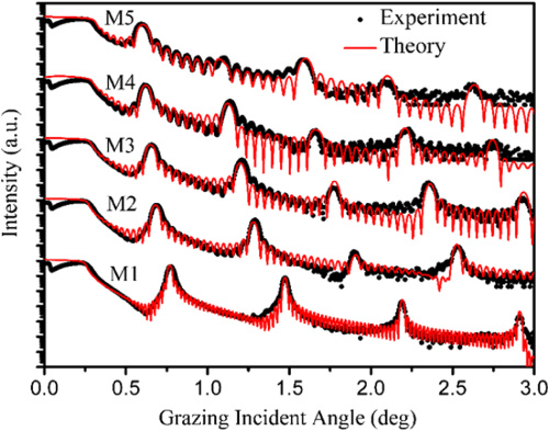
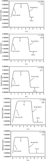
All the samples were characterized by GIXRR in the angular range of 0°–3°. In this study, the IMD [14] was used to fit the experimental data. Because the layers of the FeCo/Si multilayer diffused severely, a gradient refractive index model was used to fit the experimental data. The experimental and theoretical results are shown in Fig. 1 and are plotted as a function of the grazing incident angle. Black points represent the experimental data, and red curves represent the fitting data (theoretical data). The variation in the refractive index of the layers is shown in Fig. 2. The $x$ axis represents an arbitrary unit. Figures 2(a)–2(e) represent the five samples M1 to M5, respectively.
The fitted results obtained using the gradient refractive index model matched well with the experimental data. Figures 1 and 2 illustrate that there is severe diffusion at the interfaces of the FeCo/Si multilayer, which represent the Si-on-FeCo and FeCo-on-Si interface layers. The thickness of the FeCo-on-Si interface is larger than that of the Si-on-FeCo interface of the five samples, which demonstrates that interfacial asymmetry of the FeCo/Si multilayers always existed.
B. Transmission Electron Microscopy
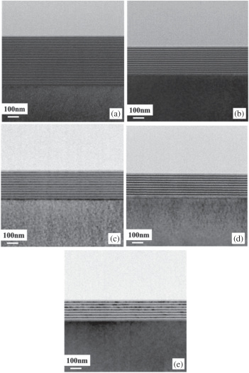
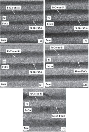
The full-view images of the five samples, including the Si substrate at the bottom and the passivation layer at the top, are shown in Fig. 3 using the bright field mode in TEM. The HRTEM images of all the samples shown in Fig. 4 represent samples M1–M5, respectively. The dark layers are FeCo, and the bright layers are Si. Severe diffusion is observed at the interface.
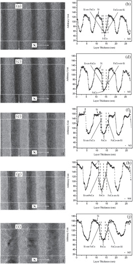
To further understand the TEM results, TEM Gatan digital micrograph software was used to extract grayscale image data. The selected area grayscale curves of all the samples are shown in Fig. 5. Figures 5(a) and 5(b) represent M1; Figs. 5(c) and 5(d) represent M2; Figs. 5(e) and 5(f) represent M3; Figs. 5(g) and 5(h) represent M4; and Figs. 5(i) and 5(j) represent M5. At the top of each curve in Fig. 5, there is a part of its corresponding HRTEM image that is rotated 90° counterclockwise. Therefore, the $x$ axis represents the direction from the air to the substrate, which is a pixel. However, the ‘pixel’ with “nm” is replaced for better understanding (${1}\;{\rm pixel} = {22}\;{\rm nm}$). The $y$ axis represents the grayscale value and color depth. The peak corresponds to the Si layer, and the trough corresponds to the FeCo layer. The 20%–80% difference between the peak and trough represents the interlayers.

Fig. 5. Selected area grayscale curves of all samples. On the top of each curve is the corresponding HRTEM image, which is rotated by 90°.
According to Fig. 5, it can be found that the left-hand area of the FeCo layer is much steeper than the right-hand area in all samples with varied FeCo layer thicknesses. Figures 4 and 5 show that there is severe interface diffusion in the FeCo/Si multilayers, and the thickness of the FeCo-on-Si interface is always larger than that of the Si-on-FeCo interface, which explains the asymmetry in the thickness of the interface layer. These results were consistent with the GIXRR measurements.
Naik et al. [8] found that the thicknesses of Fe-on-Si and Si-on-Fe interlayers were independent of the Fe and Si layer thickness. However, the thicknesses of the Fe and Si layers were both varied in Naik’s study, which was not accurate to study the effect of thickness on the interfaces. The interfacial asymmetry of Fe/Si multilayers with the increasing thickness of the Si layer has been investigated by our group [13]. The thickness of Si-on-Fe interlayers remained almost constant, but that of Fe-on-Si decreased with the increasing thickness of the Si layer. Therefore, our study aimed at the varied thickness of FeCo layers, which could better exhibit the effect of thickness of FeCo on the interface asymmetry.
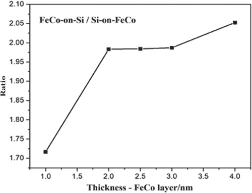
The ratio of the thickness of FeCo-on-Si and Si-on-FeCo as a function of the FeCo thickness of all FeCo/Si multilayer films was plotted in Fig. 6. The interfacial asymmetry of the FeCo/Si multilayers always existed, and exhibited an upward trend with the increasing thickness of the FeCo layer.
Fig. 6. Ratio of the thickness of FeCo-on-Si and Si-on-FeCo as a function of the FeCo thickness of all FeCo/Si multilayer films.
C. Selected Area Electron Diffraction and Transmission Electron Microscopy–Dark Field
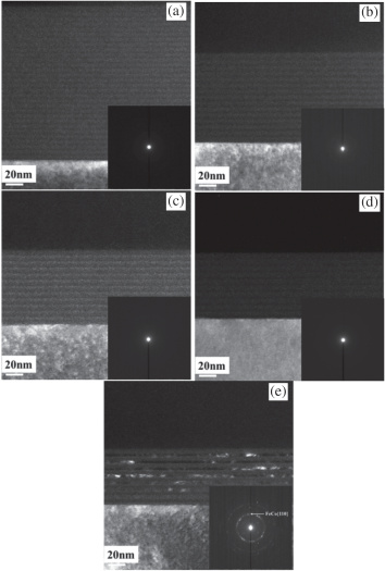
The SAED and TEM DF results of all samples are shown in Fig. 7. Figures 7(a)–7(e) represent the five samples M1–M5, respectively. The middle bright spot in the lower-right corner of Fig. 6 is the light that irradiates the detector blocked by a vertical barrier. Figure 7 shows that the FeCo layer did not crystallize from M1 to M4. However, as the thickness of the FeCo layer reached 4 nm, it changed from an amorphous to a crystalline state. The diffraction dots in the right corner of Fig. 7(e) represent FeCo {110}. These results indicate that the crystallization of FeCo was suppressed because of severe diffusion from the Si layer to the FeCo layer. Compared with the results reported in [15], the FeCo/Si multilayer fabricated by magnetron sputtering crystallizes at a larger thickness. The diffusion from the Si layer to the FeCo layer is likely more severe in magnetron sputtering than in triode sputtering, which suppresses the crystallization of FeCo.
Fig. 7. Selected area electron diffraction patterns and transmission electron microscopy–dark field results of all FeCo/Si multilayer films.
4. CONCLUSION
Five FeCo/Si multilayer films with various FeCo thicknesses were deposited using the dc-MS technique. GIXRR, HRTEM, and SAED analyses were used to examine the interfacial structures. The GIXRR results reveal that asymmetric interface diffusion layers exist in the FeCo/Si multilayer, and the thickness of the Si-on-FeCo interlayer is less than that of FeCo-on-Si. The HRTEM results provide evidence that diffusion from the Si layer to the FeCo layer is severe, and the roughness of the FeCo layer becomes large as the thickness of the FeCo layer reaches 4 nm. The SAED patterns and TEM DF results indicate that the FeCo layer partially crystallized in M5.
The difference between the FeCo-on-Si and Si-on-FeCo interface diffusion layers can be explained by the difference in the surface free energy of ${{\rm Fe}_{89}}{{\rm Co}_{11}}$ and Si, which is analogous to ${\rm Fe}\;({2.9}\;{{\rm Jm}^{- 2}})$ and ${\rm Si}\;({1.2}\;{{\rm Jm}^{- 2}})$ [16,17]. When FeCo is fabricated on a Si surface, Si atoms move more easily to the surface by a chemical driving force because of the lower surface free energy of Si and the high energy when FeCo atoms bombard the film surface. This results in severe diffusion of the FeCo-on-Si interface layer. In addition, they can produce FeSi and CoSi compounds. The severe interfacial diffusion is the main factor that restricts its application in polarized neutron supermirrors. Future research will mainly focus on inhibiting the interfacial diffusion of FeCo/Si multilayers.
Funding
National Key Research and Development Program of China (2016YFA0401304, 2017YFA0403302); National Natural Science Foundation of China (11443007, 11505129, 61621001, U1732268); National Natural Science Foundation of China Academy of Engineering Physics (U1430131); National Key Scientific Instrument and Equipment Development Projects of China (2012YQ04016403, 2012YQ13012505).
Disclosures
The authors declare no conflicts of interest.
Data availability
No data were generated or analyzed in the presented research.
REFERENCES
1. D. Pescia, R. F. Willis, and J. A. C. Bland, “Magnetic moments of ultrathin films by spin polarized neutron reflection,” Surf. Sci. 189, 724–728 (1987). [CrossRef]
2. J. P. Carbotte, E. Schachinger, and D. N. Basov, “Coupling strength of charge carriers to spin fluctuations in high-temperature superconductors,” Nature 401, 354–356 (1999). [CrossRef]
3. F. Mezei, “Novel polarized neutron devices: supermirror and spin component amplifier,” Commun. Phys. 1, 81–85 (1976).
4. M. Mâaza, M. Spegel, C. Sella, B. Pardo, A. Menelle, J. Corno, and R. Gaziel, “Thermal stability of Co–Ti multilayered neutron polarizers,” Solid State Commun. 112, 177–181 (1999). [CrossRef]
5. A. F. Schebetov, N. K. Pleshanov, V. M. Pusenkov, B. G. Peskov, G. E. Shmelev, W. H. Kraan, P. T. Por, M. Th. Rekveldt, and V. E. Mikhailova, “Construction and testing of a multichannel polariser for thermal neutrons,” Nucl. Instrum. Methods Phys. Res. B. 94, 575–580 (1994). [CrossRef]
6. D. Clemens, P. Böni, H. P. Friedli, R. Göttel, C. Fermon, H. Grimmer, H. van Swygenhoven, J. Archer, F. Klose, Th. Krist, F. Mezei, and P. Thomas, “Polarizing Ti1-uXu/(FexCoyVz) supermirrors,” Physica B 213, 942–944 (1995). [CrossRef]
7. P. Høghøj, I. Anderson, R. Siebrecht, W. Graf, and K. Ben-Saidane, “Neutron polarizing Fe/Si mirrors at ILL,” Physica B 267, 355–359 (1999). [CrossRef]
8. S. R. Naik, S. Rai, M. K. Tiwari, and G. S. Lodha, “Structural asymmetry of Si/Fe and Fe/Si interface in Fe/Si multilayers,” J. Phys. D 41, 115307 (2008). [CrossRef]
9. D. Clemens, T. Krist, P. Schubert-Bischoff, J. Hoffmann, and F. Mezei, “Structure, roughness and magnetization behaviour of triode sputtered Co11Fe89-Si multilayers,” Phys. Scr. 50, 195 (1994). [CrossRef]
10. D. J. Müller, T. Krist, P. Schubert-Bischoff, and F. Mezei, “Interface effects in FeCo-Si magnetic multilayers,” Physica B 234, 1050–1051 (1997). [CrossRef]
11. S. J. Cho, T. Krist, and F. Mezei, “Dependence of interface layer thickness in FeCo–Si multilayers on sputtering parameters,” Thin Solid Films 444, 158–164 (2003). [CrossRef]
12. S. J. Cho, T. Krist, and F. Mezei, “Determination of interface growth with atomic resolution in FeCo–Si multilayers,” Thin Solid Films 434, 136–144 (2003). [CrossRef]
13. Z. Zhang, J. J. Wang, Y. H. Lian, R. Alnaimi, Z. S. Wang, and H. Chen, “Influence of various Si layers on the interlayer thicknesses of the direct current magnetron sputtered Fe/Si multilayers,” Thin Solid Films 592, 312–317 (2015). [CrossRef]
14. D. L. Windt, “IMD Software for modeling the optical properties of multilayer films,” Comput. Phys. 12, 360–370 (1998). [CrossRef]
15. S. J. Cho, H. Y. Kang, C. H. Lee, Y. J. Kim, and T. Krist, “Crystallization and magnetic properties of FeCo/Si multilayer,” Nucl. Instrum. Methods Phys. Res. A 529, 94–97 (2004). [CrossRef]
16. A. Gupta, D. Kumar, and V. Phatak, “Asymmetric diffusion at the interfaces in Fe/Si multilayers,” Phys. Rev. B 81, 155402 (2010). [CrossRef]
17. S. M. Amir, M. Gupta, A. Gupta, K. Ambika, and J. Stahn, “Silicide layer formation in evaporated and sputtered Fe/Si multilayers: X-ray and neutron reflectivity study,” Appl. Surf. Sci. 277, 182–185 (2013). [CrossRef]