
Abstract
The wave nature of light sets a fundamental diffraction limit that challenges confinement and control of light in nanoscale structures with dimensions significantly smaller than the wavelength. Here, we study light–matter interaction in van der Waals ${{\rm MoS}_2}$ nanophotonic devices. We show that light can be coupled and guided in structures with dimensions as small as $\simeq \lambda /16$ (${\sim}{60}\;{\rm nm}$ at 1000 nm excitation wavelength), while offering unprecedented optical field confinement. This deep subwavelength optical field confinement is achieved by exploiting strong lightwave dispersion in ${{\rm MoS}_2}$. We further study the performance of a range of nanophotonic integrated devices via far- and near-field measurements. Our near-field measurements reveal detailed imaging of excitation, evolution, and guidance of fields in nanostructured ${{\rm MoS}_2}$, whereas our far-field study examines light excitation and coupling to highly confined integrated photonics. Nanophotonics at a fraction of a wavelength demonstrated here could dramatically reduce the size of integrated photonic devices and opto-electronic circuits with potential applications in optical information science and engineering.
© 2023 Optica Publishing Group under the terms of the Optica Open Access Publishing Agreement
1. INTRODUCTION
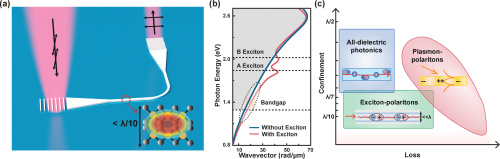
Subwavelength light coupling and manipulation [1–3] hold great promise for a wide range of science and engineering disciplines. Nanophotonics has already influenced exascale and quantum computing [4–8], photonic integrated circuits for ultra-broadband communications [9–12], efficient bio and chemical sensing [13–16], and improving climate sustainability [17,18] among others. By further bridging the gap between optical fields ($\lambda \sim 1\;{\unicode{x00B5}{\rm m}}$) and much smaller intrinsic material excitations, typically manifested at $\ll 100\;{\rm nm}$, the full potential of nanophotonics can be harnessed. Yet, coupling, guidance, and control of light in structures with deep subwavelength features ${\lt}100\;{\rm nm}$ (${\lt}\lambda /10$), to date, remains a challenge. Here, we demonstrate that electronically bulk molybdenum disulfide (${{\rm MoS}_2}$)—a layered van der Waals semiconductor in the family of transition metal dichalcogenides (TMDCs) [19–21]—enables integrated photonic devices as thin as $\simeq \lambda /16$ [Fig. 1(a)]. With the use of scattering near-field microscopy and far-field imaging, we examine properties of light guidance and coupling within a range of deeply subwavelength devices. The observed light control at the fraction of a wavelength is attributed to a unique ${{\rm MoS}_2}$ lightwave dispersion, in part driven by intrinsic coupling between excitons and photons.

Fig. 1. Deeply subwavelength photonics assisted by van der Waals materials. (a) Conceptual illustration of a ${{\rm MoS}_2}$ integrated photonic waveguide studied in this work. Light can be coupled, confined, and guided in devices thinner than $\lambda /10$. (b) Guided wave dispersion in a 60 nm thick ${{\rm MoS}_2}$ waveguide with and without exciton contribution. The shaded area corresponds to bulk bandgap where optical absorption is high. The highlighted region indicates the wavelength range studied here. (c) Conceptual comparison between different material platforms. Similar to plasmon-polaritons, photonics in excitonic materials can enable deep subwavelength devices, while offering low below-bandgap extinction.
Presently, subwavelength (${\lt}$$\lambda /2$) photonics is based on two key material avenues—dielectrics and metals. All-dielectric systems, featuring low optical extinction below the bandgap ($n \gg k$ and $k \to 0$, where $n$ is refractive index and $k$ is extinction coefficient), are very efficient at controlling light at the scale $\simeq \frac{\lambda}{{2n}}$. Such areas as photonic integrated circuits, metasurface optics, and on-chip opto-electronics have benefited from all-dielectric photonic devices [5,22–28]. However, the limited range of refractive indices [29,30] of conventional dielectrics and semiconductors (typically $n \lt 3.5$ in the near-infrared band; see Supplement 1, Section I) challenges the creation of deep subwavelength integrated photonic devices. Metals offer an alternative, where strong coupling and hybridization with bulk charge density waves drastically modify lightwave dispersion, giving rise to highly confined surface plasmon-polaritons with a high effective guide index [1,31]. The ability of these excited states to squeeze light well below the diffraction limit found a wide range of applications, from interconnects to quantum optics to photochemistry [9,12,18,32]. Nonetheless, high free electron density in metals inevitably contributes to optical loss [33,34], which narrows the range of applications for plasmonic components and devices (Supplement 1, Section I).
Light coupling to intrinsic material excitations is also naturally attained in van der Waals transition metal dichalcogenides (${{\rm MX}_2}$ compounds where ${\rm M} = {\rm Mo}$, W; ${\rm X} = {\rm S}$, Se, Te), in which excitons with large binding energies are excited [19–21,35]. Interaction of photon modes with excitons in electronically bulk TMDCs leads to hybrid waves [36–38] (extensive study and derivation of exciton–photon coupling and hybridization is provided in Supplement 1, Section I). Strong exciton–photon interaction and formation of exciton-polaritons have been examined in a number of bulk TMDCs structures [39–44]. Excitonic van der Waals materials are notable for their distinct electronic band dispersion, leading to significant optical anisotropy, high refractive index, and room temperature excitons. Exciton coupling with optical fields yields strong optical dispersion [Fig. 1(b)]. However, unlike metals suffering from free electron damping [33,34], below bandgap absorption in excitonic materials is expected to be low [45–49] [Fig. 1(b); see also Supplement 1 Figures S3 and S7], giving an opportunity to create efficient integrated photonic devices [45,49].
The utility of high refractive index bulk TMDCs has already been recognized in the design of nanoscale resonators [40,41,50–52] and metasurfaces [53,54]. Near-field measurements further revealed that hybrid exciton-polaritons could be excited and guided in exfoliated flakes of transition metal dichalcogenides [39,55]. At the same time, light coupling to integrated photonic devices made of TMDCs and wave dispersion within subwavelength nanostructures are yet to be explored. Here, for the first time to the best of our knowledge, we employ a combination of scattering near-field microscopy and far-field imaging spectroscopy to examine a range of passive integrated ${{\rm MoS}_2}$ photonic devices, including ridge waveguides, beam splitters, and interferometers. We study the performance of these devices in the vicinity of the exciton resonance and across the edge of the bulk ${{\rm MoS}_2}$ bandgap (750–1050 nm), as marked in Fig. 1(b). We demonstrate that, by utilizing strong dispersion in ${{\rm MoS}_2}$ deeply subwavelength, i.e., ${\lt}\lambda /16$, integrated photonic devices with small mode volume and device footprint [Fig. 1(a)] can be created. Deeply subwavelength light confinement in ${{\rm MoS}_2}$, and other excitonic TMDCs [21], expands the nanophotonic pallet [Fig. 1(c)].
2. RESULTS AND DISCUSSION
A. Far-Field Measurements of Deeply Subwavelength Waveguides
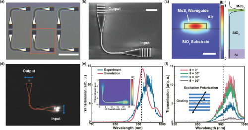
We begin with a far-field study of light coupling and propagation in a ${{\rm MoS}_2}$ waveguide [Fig. 1(a)]. Figures 2(a) and 2(b) show optical and scanning electron microscopy (SEM) images of fabricated waveguides out of a mechanically exfoliated ${{\rm MoS}_2}$ flake atop a ${{\rm SiO}_2}/{\rm Si}$ substrate (oxide layer is 2 µm thick). These structures are written using e-beam lithography with negative resist and are patterned by reactive ion etching with the hard resist as etching mask (Supplement 1, Section III). In our far-field experiments, the waveguides are excited with input and output grating couplers optimized for the 950–1000 nm wavelength band (design details are available in Supplement 1, Sections II and V). The length of fabricated waveguides is limited by the exfoliated flake size (typically ${\lt}40\;{\unicode{x00B5}{\rm m}} \times 40\;{\unicode{x00B5}{\rm m}}$ area). Therefore, in order to increase the signal contrast between the output grating coupler and overall light scattering, we design our experiments for a cross polarization far-field microscopy (Supplement 1, Section II). For this purpose, a 90° bending with a radius of 3 µm is introduced. The fabricated waveguides are 85 nm thick and 320 nm wide (measured by atomic force microscopy (AFM) and SEM; a detailed description of device fabrication and characterization, including Raman spectroscopy and energy-dispersive X-ray spectroscopy (EDS), is available in Supplement 1, Section III). The designed waveguides are single mode supporting only a single transverse electric (TE) photonic mode (polarized along the ${{\rm MoS}_2}$ crystallographic plane). The respective mode profile is shown in Fig. 2(c). Large thickness of the ${{\rm SiO}_2}$ layer and high index contrast with ${{\rm MoS}_2}$ confine the optical mode in the waveguide with minimal leakage to the substrate [Fig. 2(c)]. The calculated overall mode area, ${A_{{\rm eff}}} = \frac{{{{( \iint _{- \infty}^\infty {{| {\boldsymbol E} |}^2}\;{\rm d}x{\rm d}y)}^2}}}{{\iint _{- \infty}^\infty {{| {\boldsymbol E} |}^4}\;{\rm d}x{\rm d}y}}$, at 1 µm wavelength is ${\sim}0.053\;{{\unicode{x00B5}{\rm m}}^2}$ (${\sim}{21}\%$ of a free space diffraction-limited spot, ${A_0} = {\lambda ^2}/4$). The fabricated ${{\rm MoS}_2}$ waveguide size and respective mode area are significantly smaller than that of a corresponding optimum for a silicon waveguide (for comparison, in silicon minimum mode area of $0.072\;{{\unicode{x00B5}{\rm m}}^2}$ is attained for a 140 nm by 365 nm ridge waveguide; see also Section 2.D).
Fig. 2. Far-field study of deeply subwavelength ${{\rm MoS}_2}$ waveguides. (a) Optical micrograph of fabricated waveguides. Scale bar: 20 µm. (b) SEM image of the fabricated device. Scale bar: 4 µm. (c) Optical mode profile (left) and a related cross-section (right) at 1 µm wavelength. The height and width of the device are 85 nm and 320 nm, respectively. (d) Far-field image of the scattered light collected in cross polarized light with a contour of the device outlined by a dashed curve. The arrows indicate the polarizations of input and output beam paths. (e) Measured and simulated waveguide transmission spectra. Inset shows the simulated field profile at 960 nm. (f) Polarization dependent waveguide transmission spectra. In (e) and (f), dashed lines denote the wavelength of bulk ${{\rm MoS}_2}$ bandgap.
Upon illumination of the input coupler with the incident beam polarized along the grating [${\theta _{\rm{in}}} = {0^\circ}$ as shown in Fig. 2(f)], TE photonic mode [38,39] is excited and guided in the waveguide (Supplement 1, Section I). Figure 2(d) shows a far-field confocal microscope image collected in a cross-polarized light centered around 915 nm (1.36 eV) excitation wavelength. Respective device transmission spectra are plotted in Fig. 2(e). To understand the measurements, we perform detailed FDTD simulations [also plotted in Fig. 2(e)]. The transmission spectra are a function of the spectral responses of the grating couplers, coupling efficiency, and optical extinction in the waveguide itself. Measurements and simulations show that no light is guided and transmitted below 900 nm, which we attribute to a strong light absorption above bulk bandgap (1.29 eV) [56] and close to A exciton resonance at 670 nm (1.85 eV) [47] (Supplement 1, Sections II and V), as well as to a high index contrast, which reduces the coupling efficiency (Supplement 1, Section II). Moving closer to the band edge, optical extinction in MoS2 decreases, and grating coupler efficiency increases, making light transmission through the device possible. The observed peak in transmission spectra at ${\sim}{980}\;{\rm nm}$ is associated with the grating coupler efficiency optimum (Supplement 1, Section V). It is worth noting that, due to strong mode confinement in the waveguide core, no notable light scattering is observed at the waveguide bend despite a small bending radius. In contrast, strong scattering is seen at the taper–waveguide interface, suggesting that a better-optimized coupler geometry is needed [57].
To further verify that the fabricated waveguide is single mode and only TE photonic mode can be excited, we perform polarization-dependent spectroscopy as plotted in Fig. 2(f). Specifically, we vary incident light polarization from ${\theta _{\rm{in}}} = {0^\circ}$ to ${\theta _{\rm{in}}} = {90^\circ}$ (output light is collected at ${\theta _{\rm{out}}} = {0^\circ}$ with respect to the output coupler) and observe that light transmission is reduced, manifesting that only TE waves are guided (observed small signal at ${\theta _{\rm{in}}} = {90^\circ}$ is attributed to a light scattered by the input port). The measurement agrees well with FDTD simulations (Supplement 1, Figure S22). Supplement 1 Section VI further discusses the measurement of control devices with an input-only grating and expands on polarization-dependent waveguide excitation.
B. Near-Field Imaging of Confined Exciton-Polaritons
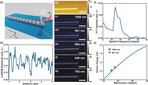
Next, to gain a better understanding of wave propagation within such deeply subwavelength ${{\rm MoS}_2}$ devices, we perform near-field nano-optical imaging of a set of straight 15 µm, 20 µm, and 25 µm long waveguides (fabricated waveguides are 80 nm thick and 300 nm wide; see Fig. 3(b) and Supplement 1, Section VII). A schematic illustration of the setup is shown in Fig. 3(a). In the experiment, we use a scattering-type scanning near-field optical microscope (s-SNOM) with a spatial resolution of ${\sim}{25}\;{\rm nm}$ (i.e., ${\sim}{12}$ points across the waveguide) [58]. Near-field imaging and spectroscopy have emerged as a powerful tool to examine the dispersion of waves in a diverse set of materials [59–62]. Prior near-field studies of wave propagation in exfoliated flakes have revealed strong exciton–photon coupling and highly anisotropic wave propagation [63,64]. At the same time, to the best of our knowledge, the near-field study of nanostructured transition metal dichalcogenide devices has not been performed yet. In the case of ${{\rm MoS}_2}$, such a measurement is challenged by a small device footprint and by a need for s-polarization for waveguide excitation (to excite the TE photon mode). These factors contribute to a weak signal contrast necessitating the careful design of the experiment.
Fig. 3. Near-field study of deeply subwavelength ${{\rm MoS}_2}$ waveguides. (a) Conceptual illustration of the setup. (b) AFM topographic map of the device. (c)–(g) s-SNOM images at wavelengths ranging from 793 nm to 1000 nm. (h) Interference fringe line profile extracted at 961 nm excitation wavelength (inset). (i) Fourier transform of the interference fringe line profile shown in panel (h). (j) Predicted and extracted TE photonic mode dispersion. Scale bar: 2 µm.
Figures 3(c)–3(g) show a set of s-SNOM images collected at various excitation wavelengths for a 15 µm long waveguide under an $s$-polarized excitation [55] [that is, the incident electric field is perpendicular to the ${{\rm MoS}_2}$ crystal axis and waveguide; Fig. 3(a)]. Similar to the far-field measurement [Fig. 2(e)], below 900 nm waves are not excited. Above 900 nm, we observe interference fringe patterns close to both edges of the waveguide, signifying that the guided TE photonic mode is excited and guided. These interference fringe patterns are generated by a superposition between light scattered directly off the s-SNOM tip and excited mode [63] (see also Supplement 1, Section VII). Note that, to extract guided wave dispersion, we perform spatial Fourier transform on collected interference fringe profiles [39,65]. Figures 3(h) and 3(i) show the s-SNOM amplitude of an interference fringe profile and a related spatial Fourier spectrum for a waveguide excited at 961 nm (1.29 eV), respectively. By tracing the peak of the Fourier spectrum, we extract the interference fringe period, $\rho$, which is related to the wavelength of the excited TE photonic mode: $\lambda = \frac{{\rho {\lambda _0}}}{{\rho \cos \alpha + {\lambda _0}}}$ (see Supplement 1, Section VII for details), where $\alpha = {30^\circ}$ is the incidence angle [Fig. 3(a)] and ${\lambda _0}$ is the excitation wavelength [63]. In Fig. 3(j), we plot theoretically predicted wave dispersion and dispersion extracted from the near-field measurement, where an excellent agreement is revealed. Note that spatial Fourier transform at 793 nm, 848 nm, and 904 nm is hindered by a small signal to noise ratio.
C. Passive Integrated van der Waals Devices
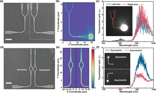
Next, to elucidate the capability of ${{\rm MoS}_2}$ for deeply subwavelength integrated nanophotonics, we perform a far-field study of several passive photonic devices. Figure 4(a) shows an SEM of a fabricated 60 nm thick (i.e., ${\lt}\lambda /16$ at 1000 nm), 360 nm wide, and ${\sim}33\;{\unicode{x00B5}{\rm m}}$ long Y-junction beam splitter (see Supplement 1, Section VIII for details). For such a small device cross-section, only a fundamental TE photonic mode can be excited. In Fig. 4(b), we plot a corresponding profile of the wave excited at $\lambda = 960\;{\rm nm}$ [Fig. 1(b) shows corresponding mode dispersion with and without exciton contribution]. A respective far-field cross-polarized confocal image is shown in the inset of Fig. 4(c). Two equally bright emission spots are observed at the output couplers (spaced 5 µm apart) of the device. Figure 4(c) shows corresponding spectra measured at both output couplers. The analysis of overall power carried in the 900 nm to 1050 nm band [i.e., $\smallint _{900}^{1050}{T_i}(\lambda){\rm d}\lambda$, where ${T_i}(\lambda)$ is the transmission spectral power density through either the left or right arm of the beam splitter] yields a 47.15/52.85 splitting ratio between the two outputs, which indicates that a nearly 50/50 splitting of optical power is attained, as designed.
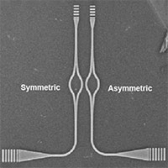
Fig. 4. Integrated exciton-driven ${{\rm MoS}_2}$ nanophotonic devices. (a) SEM image of Y-junction beam splitters. Scale bar: 5 µm. (b) Simulated field intensity for a device shown in (a) at ${\lambda} = 960{\rm \;nm}$ excitation wavelength. (c) Beam splitter transmission spectra. Inset, far-field image of the Y-splitter collected at 915 nm center wavelength. (d) SEM image of symmetric and asymmetric Mach–Zehnder interferometers. Scale bar: 5 µm. (e) Simulated field intensity for interferometers shown in (d) at ${\lambda} = 960{\rm \;nm}$. (f) Transmission spectra for symmetric and asymmetric Mach–Zehnder interferometers, respectively. Inset, far-field image of Mach–Zehnder interferometers at 915 nm center wavelength.
Based on the Y-splitter design, we further study a Mach–Zehnder interferometer. The symmetric (with equal length of arms of ${\sim}{10.41}\;\unicode{x00B5}{\rm m}$) and asymmetric (shorter arm length is ${\sim}{9.9}\;\unicode{x00B5}{\rm m}$, i.e., ${\sim}{500}\;{\rm nm}$ arm length difference) interferometer structures with an overall device length of ${\sim}40\;{\unicode{x00B5}{\rm m}}$ are designed [Fig. 4(d)]. Figure 4(e) shows respective simulations of field profiles at $\lambda = 960\;{\rm nm}$. Constructive interference in the case of a symmetric structure is clearly seen, although the overall amplitude decreases due to optical loss at this wavelength. On the other hand, the phase difference between the arms of the asymmetric device is designed to yield destructive interference at the output. We note that, due to an appreciable optical extinction at 960 nm, the two arms lead to a different insertion loss. As a result, a complete phase cancellation is not attained in the wavelength band studied here (750–1050 nm). Figure 4(f) presents a corresponding far-field study of fabricated symmetric and antisymmetric interferometers. Cross-polarization images [Fig. 4(f), inset] suggest a stronger attenuation by an antisymmetric device, as expected. The difference between symmetric and antisymmetric configuration is further seen from measured transmission spectra [Fig. 4(f)]. The observed asymmetry in transmission at ${\sim}{980}\;{\rm nm}$ excitation wavelength is more than 2 times and matches well with theoretical predictions (Supplement 1, Section VIII).
D. Confinement Figure of Merit
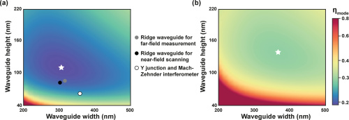
Lastly, to better understand light confinement in nanostructured ${{\rm MoS}_2}$ as compared to Si waveguides, we examine effective mode area and confinement factor. We note that the fundamental TE mode studied here is cutoff free. Indeed, waves can be excited and guided even in a 1 atom thick waveguide [66,67]. However, in this case, the optical mode is highly delocalized. It is desirable to find an optimum between mode confinement and device footprint. For this purpose, we introduce the normalized mode area, defined as ${\eta _{{\rm mode}}} = \frac{{{A_{\rm{eff}}}}}{{{A_0}}}$, and study ${\eta _{\rm{mode}}}$ as a function of device dimensions.
In Fig. 5(a), we plot normalized mode area, ${\eta _{\rm{mode}}}$, for a fundamental TE mode at $\lambda = 1\;{\unicode{x00B5}{\rm m}}$ in a ${{\rm MoS}_2}$ waveguide as a function of waveguide dimensions. For comparison, we also plot ${\eta _{\rm{mode}}}$ for fundamental TE guided mode in a Si waveguide in Fig. 5(b). Higher refractive index of ${{\rm MoS}_2}$ leads to a stronger confinement of the optical field and to smaller footprint devices, when compared with Si waveguide. With smaller and thinner devices, ${{\rm MoS}_2}$ can more efficiently confine light at a smaller effective area. The smallest mode area that can be achieved in a Si waveguide is ${\gt}{50}\%$ larger than that in a ${{\rm MoS}_2}$ waveguide (0.288 versus 0.191, respectively). At the same time, corresponding cross-section for ${{\rm MoS}_2}$ is 50% smaller than that of Si device (${110}\;{\rm nm} {\times} {305}\;{\rm nm}$ for ${{\rm MoS}_2}$ versus ${140}\;{\rm nm} {\times} {365}\;{\rm nm}$ for Si, respectively). We mark the dimensions and the corresponding normalized mode area of three ${{\rm MoS}_2}$ devices studied in this work: ridge waveguide for far-field measurement, ridge waveguide for near-field imaging, and Y-splitters and Mach–Zehnder interferometers [Fig. 5(a)]. While fabricated devices are not globally optimal, the corresponding normalized mode area for these three devices (${\sim}{0.2}$ for waveguides and ${\sim}{0.24}$ for Y-splitters and interferometers) is still smaller than the optimal value achieved for a Si waveguide (${\sim}{0.288}$). Despite a seemingly small gain in the mode area and device footprint of ${{\rm MoS}_2}$ as compared to Si, the ability to squeeze light at smaller dimensions results in a stronger light–matter interaction, whereas a smaller footprint can offer higher intergration density [46]. Both of these functions play important role in complex chip sclae architectures and have the potential to enable more sophisticated computing at a lower power.
Fig. 5. Waveguide mode area study. Normalized mode area for fundamental TE mode (a) in a ${{\rm MoS}_2}$ waveguide and (b) in a Si waveguide on ${{\rm SiO}_2}/{\rm Si}$ substrate as a function of waveguide width and thickness. Here ${\lambda} = 1{\rm \;\unicode{x00B5}{\rm m}}$. The stars in both figures correspond to the optimal (smallest) mode area achieved in ${{\rm MoS}_2}$ and Si devices, respectively. The color bar is in logarithmic scale for ease of comparison. The markers in (a) correspond to geometric dimensions of the three different fabricated devices examined in this work.
3. CONCLUSION
To conclude, we demonstrated through simulations, far-field and near-field measurements that ${{\rm MoS}_2}$, owing to its unique optical dispersion, is well suited for deeply subwavelength integrated nanophotonics. Functional devices that confine, control, and guide light in devices with dimensions ${\lt}\lambda /10$ can be crafted. While in this work we have focused on the 750–1050 nm wavelength band, the principles discussed here can be extended to a telecom band (${\gt}{1200}\;{\rm nm}$) and other excitonic van der Waals materials [21] to create low loss [45–49] deeply subwavelength integrated photonic devices [30,46]. While present demonstrations are limited by the area of exfoliated flakes, rapid progress with wafer scale growth of transition metal dichalcogenides and van der Waals heterostructures [68–71], as well as development of scalable transfer processes [72], suggests that design of wafer scale integrated photonic circuits is feasible in the near future. Further development of higher quality fabrication techniques can reduce fabrication related insertion loss and yield devices limited mainly by the material extinction coefficient, which is expected to be low across the telecom band [46]. Combined with unique electronic and optical properties of van der Waals materials, exciton-driven subwavelength systems are of great promise to expand the nanophotonics applications palette [30]. During review and production of this work, the authors became aware of a recent paper where near field imaging of TMDC waveguides is performed [73].
Funding
ACS PRF (66229-DNI6); National Science Foundation (DMR-2238691, NSF-1845009, NSF-ECCS-1708579, OIA-2033454); Breakthrough Prize Foundation; Hellman Foundation; National Aeronautics and Space Administration (80NSSC21K0954); UCLA Society of Hellman Fellows.
Acknowledgment
A.R.D. acknowledges support of UCLA Society of Hellman Fellows and partial support of the NASA NIAC Program and the Breakthrough Initiatives, a division of the Breakthrough Prize Foundation. A.M. acknowledges support by NSF. S.D. acknowledges support from NSF and ACS PRF.
Disclosures
The authors declare no conflicts of interest.
Data Availability
Data underlying the results presented in this paper are not publicly available at this time but may be obtained from the authors upon reasonable request.
Supplemental document
See Supplement 1 for supporting content.
REFERENCES
1. W. L. Barnes, A. Dereux, and T. W. Ebbesen, “Surface plasmon subwavelength optics,” Nature 424, 824–830 (2003). [CrossRef]
2. J. A. Schuller, E. S. Barnard, W. Cai, Y. C. Jun, J. S. White, and M. L. Brongersma, “Plasmonics for extreme light concentration and manipulation,” Nat. Mater. 9, 193–204 (2010). [CrossRef]
3. R. Halir, P. J. Bock, P. Cheben, A. Ortega-Moñux, C. Alonso-Ramos, J. H. Schmid, J. Lapointe, D.-X. Xu, J. G. Wangüemert-Pérez, I. Molina-Fernández, and S. Janz, “Waveguide sub-wavelength structures: a review of principles and applications,” Laser Photon. Rev. 9, 25–49 (2015). [CrossRef]
4. J. L. O’Brien, A. Furusawa, and J. Vučković, “Photonic quantum technologies,” Nat. Photonics 3, 687–695 (2009). [CrossRef]
5. X. Qiang, X. Zhou, J. Wang, C. M. Wilkes, T. Loke, S. O’Gara, L. Kling, G. D. Marshall, R. Santagati, T. C. Ralph, J. B. Wang, J. L. O’Brien, M. G. Thompson, and J. C. F. Matthews, “Large-scale silicon quantum photonics implementing arbitrary two-qubit processing,” Nat. Photonics 12, 534–539 (2018). [CrossRef]
6. J. K. George, A. Mehrabian, R. Amin, J. Meng, T. F. de Lima, A. N. Tait, B. J. Shastri, T. El-Ghazawi, P. R. Prucnal, and V. J. Sorger, “Neuromorphic photonics with electro-absorption modulators,” Opt. Express 27, 5181–5191 (2019). [CrossRef]
7. W. Bogaerts, D. Pérez, J. Capmany, D. A. Miller, J. Poon, D. Englund, F. Morichetti, and A. Melloni, “Programmable photonic circuits,” Nature 586, 207–216 (2020). [CrossRef]
8. B. J. Shastri, A. N. Tait, T. Ferreira de Lima, W. H. P. Pernice, H. Bhaskaran, C. D. Wright, and P. Prucnal, “Photonics for artificial intelligence and neuromorphic computing,” Nat. Photonics 15, 102–114 (2015). [CrossRef]
9. A. Melikyan, L. Alloatti, A. Muslija, D. Hillerkuss, P. C. Schindler, J. Li, R. Palmer, D. Korn, S. Muehlbrandt, D. Van Thourhout, B. Chen, R. Dinu, M. Sommer, C. Koos, M. Kohl, W. Freude, and J. Leuthold, “High-speed plasmonic phase modulators,” Nat. Photonics 8, 229–233 (2014). [CrossRef]
10. L. W. Luo, N. Ophir, C. P. Chen, L. H. Gabrielli, C. B. Poitras, K. Bergmen, and M. Lipson, “WDM-compatible mode-division multiplexing on a silicon chip,” Nat. Commun. 5, 3069 (2014). [CrossRef]
11. K. Liu, C. R. Ye, S. Khan, and V. J. Sorger, “Review and perspective on ultrafast wavelength-size electro-optic modulators,” Laser Photon. Rev. 9, 172–194 (2015). [CrossRef]
12. P. Cheben, R. Halir, J. H. Schmid, H. A. Atwater, and D. R. Smith, “Subwavelength integrated photonics,” Nature 560, 565–572 (2018). [CrossRef]
13. C. Wu, A. B. Khanikaev, R. Adato, N. Arju, A. A. Yanik, H. Altug, and G. Shvets, “Fano-resonant asymmetric metamaterials for ultrasensitive spectroscopy and identification of molecular monolayers,” Nat. Mater. 11, 69–75 (2012). [CrossRef]
14. M. Li, S. K. Cushing, and N. Wu, “Plasmon-enhanced optical sensors: a review,” Analyst 140, 386–406 (2015). [CrossRef]
15. A. Tittl, A. Leitis, M. Liu, F. Yesilkoy, D.-Y. Choi, D. N. Neshev, Y. S. Kivshar, and H. Altug, “Imaging-based molecular barcoding with pixelated dielectric metasurfaces,” Science 360, 1105–1109 (2018). [CrossRef]
16. M. L. Solomon, J. M. Abendroth, L. V. Poulikakos, J. Hu, and J. A. Dionne, “Fluorescence-detected circular dichroism of a chiral molecular monolayer with dielectric metasurfaces,” J. Am. Chem. Soc. 142, 18304–18309 (2020). [CrossRef]
17. D. F. Swearer, H. Zhao, L. Zhou, C. Zhang, H. Robatjazi, J. M. P. Martirez, C. M. Krauter, S. Yazdi, M. J. McClain, E. Ringe, E. A. Carter, P. Nordlander, and N. J. Halas, “Heterometallic antenna−reactor complexes for photocatalysis,” Proc. Natl. Acad. Sci. USA 113, 8916–8920 (2016). [CrossRef]
18. H. Robatjazi, H. Zhao, D. F. Swearer, N. J. Hogan, L. Zhou, A. Alabastri, M. J. McClain, P. Nordlander, and N. J. Halas, “Plasmon-induced selective carbon dioxide conversion on earth-abundant aluminum-cuprous oxide antenna-reactor nanoparticles,” Nat. Commun. 8, 27 (2017). [CrossRef]
19. Q. H. Wang, K. Kalantar-Zadeh, A. Kis, J. N. Coleman, and M. S. Strano, “Electronics and optoelectronics of two-dimensional transition metal dichalcogenides,” Nat. Nanotechnol. 7, 699–712 (2012). [CrossRef]
20. K. F. Mak and J. Shan, “Photonics and optoelectronics of 2D semiconductor transition metal dichalcogenides,” Nat. Photonics 10, 216–226 (2016). [CrossRef]
21. S. Manzeli, D. Ovchinnikov, D. Pasquier, O. V. Yazyev, and A. Kis, “2D transition metal dichalcogenides,” Nat. Rev. Mater. 2, 17033 (2017). [CrossRef]
22. A. I. Kuznetsov, A. E. Miroshnichenko, M. L. Brongersma, Y. S. Kivshar, and B. Luk’yanchuk, “Optically resonant dielectric nanostructures,” Science 354, aag2472 (2016). [CrossRef]
23. P. Genevet, F. Capasso, F. Aieta, M. Khorasaninejad, and R. Devlin, “Recent advances in planar optics: from plasmonic to dielectric metasurfaces,” Optica 4, 139–152 (2017). [CrossRef]
24. S. M. Kamali, E. Arbabi, A. Arbabi, and A. Faraon, “A review of dielectric optical metasurfaces for wavefront control,” Nanophotonics 7, 1041–1068 (2018). [CrossRef]
25. M. Smit, K. Williams, and J. van der Tol, “Past, present, and future of InP-based photonic integration,” APL Photon. 4, 050901 (2019). [CrossRef]
26. S. Y. Siew, B. Li, F. Gao, H. Y. Zheng, W. Zhang, P. Guo, S. W. Xie, A. Song, B. Dong, L. W. Luo, C. Li, X. Luo, and G. Q. Lo, “Review of silicon photonics technology and platform development,” J. Lightwave Technol. 39, 4374–4389 (2021). [CrossRef]
27. D. Zhu, L. Shao, M. Yu, R. Cheng, B. Desiatov, C. J. Xin, Y. Hu, J. Holzgrafe, S. Ghosh, A. Shams-Ansari, E. Puma, N. Sinclair, C. Reimer, M. Zhang, and M. Lončar, “Integrated photonics on thin-film lithium niobate,” Adv. Opt. Photon. 13, 242–352 (2021). [CrossRef]
28. A. Boes, L. Chang, C. Langrock, M. Yu, M. Zhang, Q. Lin, M. Lončar, M. Fejer, J. Bowers, and A. Mitchell, “Lithium niobate photonics: unlocking the electromagnetic spectrum,” Science 379, eabj4396 (2023). [CrossRef]
29. N. M. Ravindra, P. Ganapathy, and J. Choi, “Energy gap–refractive index relations in semiconductors—an overview,” Infrared Phys. Technol. 50, 21–29 (2007). [CrossRef]
30. J. B. Khurgin, “Expanding the photonic palette: exploring high index materials,” ACS Photon. 9, 743–751 (2022). [CrossRef]
31. S. A. Maier, Plasmonics: Fundamentals and Applications (Springer, 2007), Vol. 1.
32. M. S. Tame, K. McEnery, S. Özdemir, J. Lee, S. A. Maier, and M. Kim, “Quantum plasmonics,” Nat. Phys. 9, 329–340 (2013). [CrossRef]
33. J. B. Khurgin, “How to deal with the loss in plasmonics and metamaterials,” Nat. Nanotechnol. 10, 2–6 (2015). [CrossRef]
34. J. B. Khurgin, “Relative merits of phononics vs. plasmonics: the energy balance approach,” Nanophotonics 7, 305–316 (2018). [CrossRef]
35. T. Mueller and E. Malic, “Exciton physics and device application of two-dimensional transition metal dichalcogenide semiconductors,” npj 2D Mater. Appl. 2, 29 (2018). [CrossRef]
36. D. S. Dovzhenko, S. V. Ryabchuk, Y. P. Rakovich, and I. R. Nabiev, “Light–matter interaction in the strong coupling regime: configurations, conditions, and applications,” Nanoscale 10, 3589–3605 (2018). [CrossRef]
37. D. G. Baranov, M. Wersall, J. Cuadra, T. J. Antosiewicz, and T. Shegai, “Novel nanostructures and materials for strong light–matter interactions,” ACS Photon. 5, 24–42 (2018). [CrossRef]
38. A. Canales, D. G. Baranov, T. J. Antosiewicz, and T. Shegai, “Abundance of cavity-free polaritonic states in resonant materials and nanostructures,” J. Chem. Phys. 154, 024701 (2021). [CrossRef]
39. F. Hu, Y. Luan, M. Scott, J. Yan, D. Mandrus, X. Xu, and Z. Fei, “Imaging exciton–polariton transport in MoSe2 waveguides,” Nat. Photonics 11, 356–360 (2017). [CrossRef]
40. M.-E. Kleemann, R. Chikkaraddy, E. M. Alexeev, D. Kos, C. Carnegie, W. Deacon, A. C. de Pury, C. Große, B. de Nijs, J. Mertens, A. I. Tartakovskii, and J. J. Baumberg, “Strong-coupling of WSE2 in ultra-compact plasmonic nanocavities at room temperature,” Nat. Commun. 8, 1296 (2017). [CrossRef]
41. R. Verre, D. G. Baranov, B. Munkhbat, J. Cuadra, M. Käll, and T. Shegai, “Transition metal dichalcogenide nanodisks as high-index dielectric Mie nanoresonators,” Nat. Nanotechnol. 14, 679–683 (2019). [CrossRef]
42. B. Munkhbat, D. G. Baranov, M. Stührenberg, M. Wersäll, A. Bisht, and T. Shegai, “Self-hybridized exciton-polaritons in multilayers of transition metal dichalcogenides for efficient light absorption,” ACS Photon. 6, 139–147 (2019). [CrossRef]
43. H. Zhang, B. Abhiraman, Q. Zhang, J. Miao, K. Jo, S. Roccasecca, M. W. Knight, A. R. Davoyan, and D. Jariwala, “Hybrid exciton-plasmon-polaritons in van der waals semiconductor gratings,” Nat. Commun. 11, 3552 (2020). [CrossRef]
44. J. Li, K. Yao, Y. Huang, J. Fang, P. S. Kollipara, D. E. Fan, and Y. Zheng, “Tunable strong coupling in transition metal dichalcogenide nanowires,” Adv. Mater. 34, 2200656 (2022). [CrossRef]
45. G. A. Ermolaev, Y. V. Stebunov, A. A. Vyshnevyy, D. E. Tatarkin, D. I. Yakubovsky, S. M. Novikov, D. G. Baranov, T. Shegai, A. Y. Nikitin, A. V. Arsenin, and V. S. Volkov, “Broadband optical properties of monolayer and bulk MoS2,” npj 2D Mater. Appl. 4, 21 (2020). [CrossRef]
46. H. Ling, R. Li, and A. R. Davoyan, “All van der waals integrated nanophotonics with bulk transition metal dichalcogenides,” ACS Photon. 8, 721–730 (2021). [CrossRef]
47. G. Ermolaev, D. Grudinin, Y. Stebunov, K. V. Voronin, V. Kravets, J. Duan, A. Mazitov, G. Tselikov, A. Bylinkin, and D. J. N. Yakubovsky, “Giant optical anisotropy in transition metal dichalcogenides for next-generation photonics,” Nat. Commun. 12, 854 (2021). [CrossRef]
48. B. Munkhbat, P. Wróbel, T. J. Antosiewicz, and T. O. Shegai, “Optical constants of several multilayer transition metal dichalcogenides measured by spectroscopic ellipsometry in the 300–1700 nm range: high index, anisotropy, and hyperbolicity,” ACS Photon. 9, 2398–2407 (2022). [CrossRef]
49. B. Munkhbat, B. Küçüköz, D. G. Baranov, T. J. Antosiewicz, and T. O. Shegai, “Nanostructured transition metal dichalcogenide multilayers for advanced nanophotonics,” Laser Photon. Rev. 17, 2200057 (2023). [CrossRef]
50. T. D. Green, D. G. Baranov, B. Munkhbat, R. Verre, T. Shegai, and M. Käll, “Optical material anisotropy in high-index transition metal dichalcogenide Mie nanoresonators,” Optica 7, 680–686 (2020). [CrossRef]
51. G. I. Tselikov, G. A. Ermolaev, A. A. Popov, G. V. Tikhonowski, D. A. Panova, A. S. Taradin, A. A. Vyshnevyy, A. V. Syuy, S. M. Klimentov, S. M. Novikov, A. B. Evlyukhin, A. V. Kabashin, A. V. Arsenin, K. S. Novoselov, and V. S. Volkov, “Transition metal dichalcogenide nanospheres for high-refractive-index nanophotonics and biomedical theranostics,” Proc. Natl. Acad. Sci. USA 119, e2208830119 (2022). [CrossRef]
52. A. A. Popkova, I. M. Antropov, G. I. Tselikov, G. A. Ermolaev, I. Ozerov, R. V. Kirtaev, S. M. Novikov, A. B. Evlyukhin, A. V. Arsenin, V. O. Bessonov, V. S. Volkov, and A. A. Fedyanin, “Nonlinear exciton-Mie coupling in transition metal dichalcogenide nanoresonators,” Laser Photon. Rev. 16, 2100604 (2022). [CrossRef]
53. C. H. Liu, J. Zheng, S. Colburn, T. K. Fryett, Y. Chen, X. Xu, and A. Majumdar, “Ultrathin van der waals metalenses,” Nano Lett. 18, 6961–6966 (2018). [CrossRef]
54. M. Nauman, J. Yan, D. de Ceglia, M. Rahmani, K. Zangeneh Kamali, C. De Angelis, A. E. Miroshnichenko, Y. Lu, and D. N. Neshev, “Tunable unidirectional nonlinear emission from transition-metal-dichalcogenide metasurfaces,” Nat. Commun. 12, 5597 (2021). [CrossRef]
55. F. Hu, Y. Luan, J. Speltz, D. Zhong, C. Liu, J. Yan, D. Mandrus, X. Xu, and Z. Fei, “Imaging propagative exciton polaritons in atomically thin WSe2 waveguides,” Phys. Rev. B 100, 121301 (2019). [CrossRef]
56. K. F. Mak, C. Lee, J. Hone, J. Shan, and T. F. Heinz, “Atomically thin MoS2: a new direct-gap semiconductor,” Phys. Rev. Lett. 105, 136805 (2010). [CrossRef]
57. A. Michaels and E. Yablonovitch, “Inverse design of near unity efficiency perfectly vertical grating couplers,” Opt. Express 26, 4766–4779 (2018). [CrossRef]
58. J. M. Atkin, S. Berweger, A. C. Jones, and M. B. Raschke, “Nano-optical imaging and spectroscopy of order, phases, and domains in complex solids,” Adv. Phys. 61, 745–842 (2012). [CrossRef]
59. S. Dai, Z. Fei, Q. Ma, A. S. Rodin, M. Wagner, A. S. McLeod, M. K. Liu, W. Gannett, W. Regan, K. Watanabe, T. Taniguchi, M. Thiemens, G. Dominguez, A. H. C. Neto, A. Zettl, F. Keilmann, P. Jarillo-Herrero, M. M. Fogler, and D. N. Basov, “Tunable phonon polaritons in atomically thin van der waals crystals of boron nitride,” Science 343, 1125–1129 (2014). [CrossRef]
60. D. N. Basov, M. M. Fogler, and F. J. García de Abajo, “Polaritons in van der Waals materials,” Science 354, aag1992 (2016). [CrossRef]
61. G. Hu, J. Shen, C.-W. Qiu, A. Alù, and S. Dai, “Phonon polaritons and hyperbolic response in van der Waals materials,” Adv. Opt. Mater. 8, 1901393 (2020). [CrossRef]
62. M. Chen, X. Lin, T. H. Dinh, Z. Zheng, J. Shen, Q. Ma, H. Chen, P. Jarillo-Herrero, and S. Dai, “Configurable phonon polaritons in twisted α-MoO3,” Nat. Mater. 19, 1307–1311 (2020). [CrossRef]
63. D. Hu, K. Chen, X. Chen, X. Guo, M. Liu, and Q. Dai, “Tunable modal birefringence in a low-loss van der Waals waveguide,” Adv. Mater. 31, 1807788 (2019). [CrossRef]
64. F. Mooshammer, S. Chae, S. Zhang, Y. Shao, S. Qiu, A. Rajendran, A. J. Sternbach, D. J. Rizzo, X. Zhu, P. J. Schuck, J. Hone, and D. N. Basov, “In-plane anisotropy in biaxial ReS2 crystals probed by nano-optical imaging of waveguide modes,” ACS Photon. 9, 443–451 (2022). [CrossRef]
65. S. Dai, Q. Ma, T. Andersen, A. S. McLeod, Z. Fei, K. M. Liu, M. Wagner, K. Watanabe, T. Taniguchi, M. Thiemens, F. Keilmann, P. Jarillo-Herrero, M. M. Fogler, and D. N. Basov, “Subdiffractional focusing and guiding of polaritonic rays in a natural hyperbolic material,” Nat. Commun. 6, 6963 (2015). [CrossRef]
66. X. Zhang, C. De-Eknamkul, J. Gu, A. L. Boehmke, V. M. Menon, J. Khurgin, and E. Cubukcu, “Guiding of visible photons at the Ångström thickness limit,” Nat. Nanotechnol. 14, 844 (2019). [CrossRef]
67. M. Lee, H. Hong, J. Yu, F. Mujid, A. Ye, C. Liang, and J. Park, “Wafer-scale δ waveguides for integrated two-dimensional photonics,” Science 381, 648–653 (2023). [CrossRef]
68. K. Ludwiczak, A. K. Dąbrowska, J. Binder, M. Tokarczyk, J. Iwański, B. Kurowska, J. Turczyński, G. Kowalski, R. Bożek, R. Stȩpniewski, W. Pacuski, and A. Wysmołek, “Heteroepitaxial growth of high optical quality, wafer-scale van der Waals heterostrucutres,” ACS Appl. Mater. Interfaces 13, 47904–47911 (2021). [CrossRef]
69. G. Jin, C.-S. Lee, X. Liao, J. Kim, Z. Wang, O. F. N. Okello, B. Park, J. Park, C. Han, H. Heo, J. Kim, S. H. Oh, S.-Y. Choi, H. Park, and M.-H. Jo, “Atomically thin three-dimensional membranes of van der Waals semiconductors by wafer-scale growth,” Sci. Adv. 5, eaaw3180 (2019). [CrossRef]
70. Q. Wang, J. Tang, and X. Li, “Layer-by-layer epitaxy of multi-layer MoS2 wafers,” Natl. Sci. Rev. 9, nwac077 (2022). [CrossRef]
71. J. Yang, Y. Gu, E. Lee, H. Lee, S. H. Park, M.-H. Cho, Y. H. Kim, Y.-H. Kimad, and H. Kim, “Wafer-scale synthesis of thickness-controllable MoS2 films via solution-processing using a dimethylformamide/n-butylamine/2-aminoethanol solvent system,” Nanoscale 7, 9311–9319 (2015). [CrossRef]
72. P. Kumar, J. Lynch, B. Song, et al., “Light–matter coupling in large-area van der Waals superlattices,” Nat. Nanotechnol. 17, 182–189 (2022). [CrossRef]
73. A. A. Vyshnevyy, G. A. Ermolaev, D. V. Grudinin, et al., "van der Waals materials for overcoming fundamental limitations in photonic integrated circuitry," Nano Lett. 23, 8057 (2023). [CrossRef]